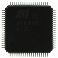
UPSD3433EB40U6 STMicroelectronics, UPSD3433EB40U6 Datasheet - Page 138

UPSD3433EB40U6
Manufacturer Part Number
UPSD3433EB40U6
Description
MCU 8BIT 8032 128KB FLASH 80TQFP
Manufacturer
STMicroelectronics
Series
µPSDr
Datasheet
1.UPSD3434EB40T6.pdf
(293 pages)
Specifications of UPSD3433EB40U6
Core Processor
8032
Core Size
8-Bit
Speed
40MHz
Connectivity
I²C, IrDA, SPI, UART/USART, USB
Peripherals
LVD, POR, PWM, WDT
Number Of I /o
46
Program Memory Size
160KB (160K x 8)
Program Memory Type
FLASH
Ram Size
8K x 8
Voltage - Supply (vcc/vdd)
3 V ~ 5.5 V
Data Converters
A/D 8x10b
Oscillator Type
Internal
Operating Temperature
-40°C ~ 85°C
Package / Case
80-TQFP, 80-VQFP
For Use With
497-5518 - EVAL BOARD RFID READER497-5046 - KIT TOOL FOR ST7/UPSD/STR7 MCU
Lead Free Status / RoHS Status
Lead free / RoHS Compliant
Eeprom Size
-
Other names
497-5660
Available stocks
Company
Part Number
Manufacturer
Quantity
Price
Company:
Part Number:
UPSD3433EB40U6
Manufacturer:
STMicroelectronics
Quantity:
10 000
- Current page: 138 of 293
- Download datasheet (5Mb)
SPI (synchronous peripheral interface)
24.5
138/293
Figure 48. SPI interface, master mode only
SPI configuration
The SPI interface is reset by the MCU reset, and firmware needs to initialize the SFRs
SPICON0, SPICON1, and SPICLKD to define several operation parameters.
The SPO Bit in SPICON0 determines the clock polarity. When SPO is set to '0,' a data bit is
transmitted on SPITxD from one rising edge of SPICLK to the next and is guaranteed to be
valid during the falling edge of SPICLK. When SPO is set to '1,' a data bit is transmitted on
SPITxD from one falling edge of SPICLK to the next and is guaranteed to be valid during the
rising edge of SPICLK. The uPSD34xx will sample received data on the appropriate edge of
SPICLK as determined by SPO. The effect of the SPO Bit can be seen in
Figure 47 on page
The FLSB Bit in SPICON0 determines the bit order while transmitting and receiving the 8-bit
data. When FLSB is '0,' the 8-bit data is transferred in order from MSB (first) to LSB (last).
When FLSB Bit is set to '1,' the data is transferred in order from LSB (first) to MSB (last).
The clock signal generated on SPICLK is derived from the internal PERIPH_CLK signal.
PERIPH_CLK always operates at the frequency, f
stopped in MCU Power Down mode. SPICLK is a result of dividing PERIPH_CLK by a sum
of different divisors selected by the value contained in the SPICLKD register. The default
value in SPICLKD after a reset divides PERIPH_CLK by a factor of 4. The bits in SPICLKD
can be set to provide resulting divisor values in of sums of multiples of 4, such as 4, 8, 12,
PERIPH_CLK
(f OSC )
INTR
8032
to
8
CLOCK
DIVIDE
SPISTAT - STATUS REGISTER
137.
SPICLKD - DIVIDE SELECT
- CONTROL REGISTERS
TIMING AND CONTROL
SPICON0, SPICON1
128
16
32
64
1
4
8
8
8
GENERATE
CLOCK
8032 MCU DATA BUS
OSC
SPITDR - TRANSMIT REGISTER
SPIRDR - RECEIVE REGISTER
, and runs constantly except when
8-bit SHIFT REGISTER
8
8
8
8
SPISEL / P1.7 or P4.7
SPICLK / P1.4 or P4.4
SPITxD / P1.6 or P4.6
Figure 46
P1.5 or P4.5
SPIRxD /
uPSD34xx
and
AI10486
Related parts for UPSD3433EB40U6
Image
Part Number
Description
Manufacturer
Datasheet
Request
R

Part Number:
Description:
MCU 8BIT 8032 128KB FLASH 80TQFP
Manufacturer:
STMicroelectronics
Datasheet:

Part Number:
Description:
MCU 8BIT 8032 128KB FLASH 52TQFP
Manufacturer:
STMicroelectronics
Datasheet:

Part Number:
Description:
STMicroelectronics [RIPPLE-CARRY BINARY COUNTER/DIVIDERS]
Manufacturer:
STMicroelectronics
Datasheet:

Part Number:
Description:
STMicroelectronics [LIQUID-CRYSTAL DISPLAY DRIVERS]
Manufacturer:
STMicroelectronics
Datasheet:

Part Number:
Description:
BOARD EVAL FOR MEMS SENSORS
Manufacturer:
STMicroelectronics
Datasheet:

Part Number:
Description:
NPN TRANSISTOR POWER MODULE
Manufacturer:
STMicroelectronics
Datasheet:

Part Number:
Description:
TURBOSWITCH ULTRA-FAST HIGH VOLTAGE DIODE
Manufacturer:
STMicroelectronics
Datasheet:

Part Number:
Description:
Manufacturer:
STMicroelectronics
Datasheet:

Part Number:
Description:
DIODE / SCR MODULE
Manufacturer:
STMicroelectronics
Datasheet:

Part Number:
Description:
DIODE / SCR MODULE
Manufacturer:
STMicroelectronics
Datasheet:

Part Number:
Description:
Search -----> STE16N100
Manufacturer:
STMicroelectronics
Datasheet:

Part Number:
Description:
Search ---> STE53NA50
Manufacturer:
STMicroelectronics
Datasheet:


