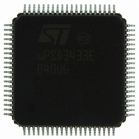
UPSD3433EB40U6 STMicroelectronics, UPSD3433EB40U6 Datasheet - Page 233

UPSD3433EB40U6
Manufacturer Part Number
UPSD3433EB40U6
Description
MCU 8BIT 8032 128KB FLASH 80TQFP
Manufacturer
STMicroelectronics
Series
µPSDr
Datasheet
1.UPSD3434EB40T6.pdf
(293 pages)
Specifications of UPSD3433EB40U6
Core Processor
8032
Core Size
8-Bit
Speed
40MHz
Connectivity
I²C, IrDA, SPI, UART/USART, USB
Peripherals
LVD, POR, PWM, WDT
Number Of I /o
46
Program Memory Size
160KB (160K x 8)
Program Memory Type
FLASH
Ram Size
8K x 8
Voltage - Supply (vcc/vdd)
3 V ~ 5.5 V
Data Converters
A/D 8x10b
Oscillator Type
Internal
Operating Temperature
-40°C ~ 85°C
Package / Case
80-TQFP, 80-VQFP
For Use With
497-5518 - EVAL BOARD RFID READER497-5046 - KIT TOOL FOR ST7/UPSD/STR7 MCU
Lead Free Status / RoHS Status
Lead free / RoHS Compliant
Eeprom Size
-
Other names
497-5660
Available stocks
Company
Part Number
Manufacturer
Quantity
Price
Company:
Part Number:
UPSD3433EB40U6
Manufacturer:
STMicroelectronics
Quantity:
10 000
- Current page: 233 of 293
- Download datasheet (5Mb)
uPSD34xx
Note:
28.5.40
Note:
2
1
Table 135. Latched address output, port B contro register (address = csiop + offset
For each bit, 1 = drive demuxed 8032 address signal on pin, 0 = pin is default mode, MCU
I/O
Default state for register is 00h after reset or power-up
Peripheral I/O mode
This mode will provide a data bus repeater function for the 8032 to interface with external
parallel peripherals. The mode is only available on Port A (80-pin devices only) and the data
bus signals, D0 - D7, are de-multiplexed (no address A0-A7). When active, this mode
behaves like a bidirectional buffer, with the direction automatically controlled by the 8032 RD
and WR signals for a specified address range. The DPLD signals PSEL0 and PSEL1
determine this address range.
mode on the Output Enable logic of the tri-state output driver for a single port pin.
on page 233
function “Peripheral I/O Mode” in PSDsoft Express on any Port A pin (all eight pins of Port A
will automatically change to this mode). Next in PSDsoft, specify an address range for the
PSELx signals in the “Chip-Select” section of the “Design Assistant”. The user can specify
an address range for either PSEL0 or PSEL1. Always qualify the PSELx equation with
“PSEN is logic '1'” to ensure Peripheral I/O mode is only active during 8032 data cycles, not
code cycles. Only one equation is needed since PSELx signals are OR’ed together
(Figure
register, Bit 7 (PIO_EN) as shown in
automatically perform this repeater function whenever the 8032 presents an address (and
memory page number, if paging is used) that is within the range specified by PSELx. Once
Port A is designated as Peripheral I/O mode in PSDsoft Express, it cannot be used for other
functions.
The user can alternatively connect an external parallel peripheral to the standard 8032 AD0-
AD7 pins on an 80-pin uPSD device (not Port A), but these pins have multiplexed address
and data signals, with a weaker fanout drive capability.
Figure 84. Peripheral I/O mode
(addr A7 or
Bit 7
A15)
PB7
VM REGISTER BIT 7 (PIO EN)
84). Then in the 8032 initialization firmware, a logic ’1’ is written to the csiop VM
8032 WR
8032 RD
PSEL0
PSEL1
03h)l
(addr A6 or
illustrates data repeater the operation. To activate this mode, choose the pin
Bit 6
A14)
PB6
(addr A5 or
Bit 5
A13)
PB5
Figure 80 on page 226
(addr A4 or
Table 99 on page
Bit 4
A12)
PB4
(DE-MUXED)
BUS D0-D7
(addr A3 or
8032 DATA
Bit 3
A11)
PB3
shows the action of Peripheral I/O
184. After this, Port A will
8
(Addr A2 or
Bit 2
A10)
PB2
(addr A1 or
Bit 1
8
PB1
A9)
PA0 - PA7
A pins
PORT
AI02886A
PSD module
Figure 84
(addr A0 or
Bit 0
233/293
PB0
A8)
Related parts for UPSD3433EB40U6
Image
Part Number
Description
Manufacturer
Datasheet
Request
R

Part Number:
Description:
MCU 8BIT 8032 128KB FLASH 80TQFP
Manufacturer:
STMicroelectronics
Datasheet:

Part Number:
Description:
MCU 8BIT 8032 128KB FLASH 52TQFP
Manufacturer:
STMicroelectronics
Datasheet:

Part Number:
Description:
STMicroelectronics [RIPPLE-CARRY BINARY COUNTER/DIVIDERS]
Manufacturer:
STMicroelectronics
Datasheet:

Part Number:
Description:
STMicroelectronics [LIQUID-CRYSTAL DISPLAY DRIVERS]
Manufacturer:
STMicroelectronics
Datasheet:

Part Number:
Description:
BOARD EVAL FOR MEMS SENSORS
Manufacturer:
STMicroelectronics
Datasheet:

Part Number:
Description:
NPN TRANSISTOR POWER MODULE
Manufacturer:
STMicroelectronics
Datasheet:

Part Number:
Description:
TURBOSWITCH ULTRA-FAST HIGH VOLTAGE DIODE
Manufacturer:
STMicroelectronics
Datasheet:

Part Number:
Description:
Manufacturer:
STMicroelectronics
Datasheet:

Part Number:
Description:
DIODE / SCR MODULE
Manufacturer:
STMicroelectronics
Datasheet:

Part Number:
Description:
DIODE / SCR MODULE
Manufacturer:
STMicroelectronics
Datasheet:

Part Number:
Description:
Search -----> STE16N100
Manufacturer:
STMicroelectronics
Datasheet:

Part Number:
Description:
Search ---> STE53NA50
Manufacturer:
STMicroelectronics
Datasheet:


