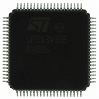
UPSD3433EB40U6 STMicroelectronics, UPSD3433EB40U6 Datasheet - Page 250

UPSD3433EB40U6
Manufacturer Part Number
UPSD3433EB40U6
Description
MCU 8BIT 8032 128KB FLASH 80TQFP
Manufacturer
STMicroelectronics
Series
µPSDr
Datasheet
1.UPSD3434EB40T6.pdf
(293 pages)
Specifications of UPSD3433EB40U6
Core Processor
8032
Core Size
8-Bit
Speed
40MHz
Connectivity
I²C, IrDA, SPI, UART/USART, USB
Peripherals
LVD, POR, PWM, WDT
Number Of I /o
46
Program Memory Size
160KB (160K x 8)
Program Memory Type
FLASH
Ram Size
8K x 8
Voltage - Supply (vcc/vdd)
3 V ~ 5.5 V
Data Converters
A/D 8x10b
Oscillator Type
Internal
Operating Temperature
-40°C ~ 85°C
Package / Case
80-TQFP, 80-VQFP
For Use With
497-5518 - EVAL BOARD RFID READER497-5046 - KIT TOOL FOR ST7/UPSD/STR7 MCU
Lead Free Status / RoHS Status
Lead free / RoHS Compliant
Eeprom Size
-
Other names
497-5660
Available stocks
Company
Part Number
Manufacturer
Quantity
Price
Company:
Part Number:
UPSD3433EB40U6
Manufacturer:
STMicroelectronics
Quantity:
10 000
- Current page: 250 of 293
- Download datasheet (5Mb)
PSD module
28.5.62
28.6
250/293
specified as “Common Clock Input, CLKIN” before programming the device with JTAG to get
the CLKIN function.
Bit 4 of PMMR0 can be set to logic ’1’ to block CLKIN from reaching the PLD input bus, but
CLKIN will still reach the APD counter.
Bit 5 of PMMR0 can be set to logic ’1’ to block CLKIN from reaching the OMC flip-flops only,
but CLKIN is still available to the PLD input bus and the APD counter.
See
SRAM standby mode (battery backup)
The SRAM on the PSD Module may optionally be backed up by an external battery (or other
DC source) to make its contents non-volatile. This is achieved by connecting a battery to pin
PC2 on Port C and selecting the “SRAM Standby” function for pin PC2 within PSDsoft
Express. Automatic voltage supply cross-over circuitry is built into the PSD Module to switch
SRAM supply to battery as soon as V
contents are protected while battery voltage is greater than 2.0V. Pin PC4 on Port C can be
used as an output to indicate that a battery switch-over has occurred. This is configured in
PSDsoft Express by selecting the “Standby On Indicator” option for pin PC4.
PSD module reset conditions
The PSD Module receives a reset signal from the MCU Module. This reset signal is referred
to as the “RST” input in PSD Module documentation, and it is active-low when asserted. The
character of the RST signal generated from the MCU Module is described in
Supervisory functions on page
Upon power-up, and while RST is asserted, the PSD Module immediately loads its
configuration from non-volatile bits to configure the PLDs and other items. PLD logic is
operational and ready for use well before RST is de-asserted. The state of PLD outputs are
determined by equations specified in PSDsoft Express.
The Flash memories are reset to Read Array mode after any assertion of RST (even if a
program or erase operation is occurring).
Flash memory WRITE operations are automatically prevented while V
it rises above the V
are allowed.
Once the uPSD34xx is up and running, any subsequent reset operation is referred to as a
warm reset, until power is turned off again. Some PSD Module functions are reset in
different ways depending if the reset condition was caused from a power-up reset or a warm
reset.
power-up and warm resets, as well as the affect of PSD Module power-down mode (from
APD).
The I/O pins of PSD Module Ports A, B, C, and D do not have weak internal pull-ups.
In MCU I/O mode, Latched Address Out mode, and Peripheral I/O mode, the pins of Ports
A, B, C, and D become standard CMOS inputs during a reset condition. If no external
devices are driving these pins during reset, then these inputs may float and draw excessive
current. If low power consumption is critical during reset, then these floating inputs should
be pulled up externally to V
Table 144 on page 243
Table 148 on page 251
LKO
voltage threshold at which time Flash memory WRITE operations
DD
for details.
summarizes how PSD Module functions are affected by
with a weak (100KΩ minimum) resistor.
83.
DD
drops below the voltage level of the battery. SRAM
DD
is ramping up until
Section 19:
uPSD34xx
Related parts for UPSD3433EB40U6
Image
Part Number
Description
Manufacturer
Datasheet
Request
R

Part Number:
Description:
MCU 8BIT 8032 128KB FLASH 80TQFP
Manufacturer:
STMicroelectronics
Datasheet:

Part Number:
Description:
MCU 8BIT 8032 128KB FLASH 52TQFP
Manufacturer:
STMicroelectronics
Datasheet:

Part Number:
Description:
STMicroelectronics [RIPPLE-CARRY BINARY COUNTER/DIVIDERS]
Manufacturer:
STMicroelectronics
Datasheet:

Part Number:
Description:
STMicroelectronics [LIQUID-CRYSTAL DISPLAY DRIVERS]
Manufacturer:
STMicroelectronics
Datasheet:

Part Number:
Description:
BOARD EVAL FOR MEMS SENSORS
Manufacturer:
STMicroelectronics
Datasheet:

Part Number:
Description:
NPN TRANSISTOR POWER MODULE
Manufacturer:
STMicroelectronics
Datasheet:

Part Number:
Description:
TURBOSWITCH ULTRA-FAST HIGH VOLTAGE DIODE
Manufacturer:
STMicroelectronics
Datasheet:

Part Number:
Description:
Manufacturer:
STMicroelectronics
Datasheet:

Part Number:
Description:
DIODE / SCR MODULE
Manufacturer:
STMicroelectronics
Datasheet:

Part Number:
Description:
DIODE / SCR MODULE
Manufacturer:
STMicroelectronics
Datasheet:

Part Number:
Description:
Search -----> STE16N100
Manufacturer:
STMicroelectronics
Datasheet:

Part Number:
Description:
Search ---> STE53NA50
Manufacturer:
STMicroelectronics
Datasheet:


