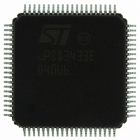
UPSD3433EB40U6 STMicroelectronics, UPSD3433EB40U6 Datasheet - Page 106

UPSD3433EB40U6
Manufacturer Part Number
UPSD3433EB40U6
Description
MCU 8BIT 8032 128KB FLASH 80TQFP
Manufacturer
STMicroelectronics
Series
µPSDr
Datasheet
1.UPSD3434EB40T6.pdf
(293 pages)
Specifications of UPSD3433EB40U6
Core Processor
8032
Core Size
8-Bit
Speed
40MHz
Connectivity
I²C, IrDA, SPI, UART/USART, USB
Peripherals
LVD, POR, PWM, WDT
Number Of I /o
46
Program Memory Size
160KB (160K x 8)
Program Memory Type
FLASH
Ram Size
8K x 8
Voltage - Supply (vcc/vdd)
3 V ~ 5.5 V
Data Converters
A/D 8x10b
Oscillator Type
Internal
Operating Temperature
-40°C ~ 85°C
Package / Case
80-TQFP, 80-VQFP
For Use With
497-5518 - EVAL BOARD RFID READER497-5046 - KIT TOOL FOR ST7/UPSD/STR7 MCU
Lead Free Status / RoHS Status
Lead free / RoHS Compliant
Eeprom Size
-
Other names
497-5660
Available stocks
Company
Part Number
Manufacturer
Quantity
Price
Company:
Part Number:
UPSD3433EB40U6
Manufacturer:
STMicroelectronics
Quantity:
10 000
- Current page: 106 of 293
- Download datasheet (5Mb)
Serial UART interfaces
106/293
of the MCU the machine cycle following the next rollover in the divide-by-16 counter. Thus,
the bit times are synchronized to the divide-by-16 counter, not to the writing of SBUF.
Transmission begins with activation of SEND which puts the start bit at pin TxD. One bit time
later, DATA is activated, which enables the output bit of the transmit shift register to pin TxD.
The first shift pulse occurs one bit time after that. As data bits shift out to the right, zeros are
clocked in from the left. When the MSB of the data byte is at the output position of the shift
register, then the 1 that was initially loaded into the 9th position is just to the left of the MSB,
and all positions to the left of that contain zeros. This condition flags the TX Control unit to
do one last shift and then deactivates SEND, and sets the interrupt flag, TI. This occurs at
the 10th divide-by-16 rollover after a write to SBUF.
Reception is initiated by a detected 1-to-0 transition at the pin RxD. For this purpose RxD is
sampled at a rate of 16 times whatever baud rate has been established. When a transition is
detected, the divide-by-16 counter is immediately reset, and 1FFH is written into the input
shift register. Resetting the divide-by-16 counter aligns its rollovers with the boundaries of
the incoming bit times. The 16 states of the counter divide each bit time into 16ths. At the
7th, 8th, and 9th counter states of each bit time, the bit detector samples the value of RxD.
The value accepted is the value that was seen in at least 2 of the 3 samples. This is done for
noise rejection. If the value accepted during the first bit time is not '0,' the receive circuits are
reset and the unit goes back to looking for another '1'-to-'0' transition. This is to provide
rejection of false start bits. If the start bit proves valid, it is shifted into the input shift register,
and reception of the reset of the rest of the frame will proceed. As data bits come in from the
right, '1s' shift out to the left. When the start bit arrives at the left-most position in the shift
register (which in mode 1 is a 9-bit register), it flags the RX Control unit to do one last shift,
load SBUF and RB8, and set the receive interrupt flag RI. The signal to load SBUF and
RB8, and to set RI, will be generated if, and only if, the following conditions are met at the
time the final shift pulse is generated:
1. RI = 0, and
2. Either SM2 = 0, or the received stop bit = 1.
If either of these two conditions are not met, the received frame is irretrievably lost. If both
conditions are met, the stop bit goes into RB8, the 8 data bits go into SBUF, and RI is
activated. At this time, whether the above conditions are met or not, the unit goes back to
looking for a '1'-to-'0' transition on pin RxD.
uPSD34xx
Related parts for UPSD3433EB40U6
Image
Part Number
Description
Manufacturer
Datasheet
Request
R

Part Number:
Description:
MCU 8BIT 8032 128KB FLASH 80TQFP
Manufacturer:
STMicroelectronics
Datasheet:

Part Number:
Description:
MCU 8BIT 8032 128KB FLASH 52TQFP
Manufacturer:
STMicroelectronics
Datasheet:

Part Number:
Description:
STMicroelectronics [RIPPLE-CARRY BINARY COUNTER/DIVIDERS]
Manufacturer:
STMicroelectronics
Datasheet:

Part Number:
Description:
STMicroelectronics [LIQUID-CRYSTAL DISPLAY DRIVERS]
Manufacturer:
STMicroelectronics
Datasheet:

Part Number:
Description:
BOARD EVAL FOR MEMS SENSORS
Manufacturer:
STMicroelectronics
Datasheet:

Part Number:
Description:
NPN TRANSISTOR POWER MODULE
Manufacturer:
STMicroelectronics
Datasheet:

Part Number:
Description:
TURBOSWITCH ULTRA-FAST HIGH VOLTAGE DIODE
Manufacturer:
STMicroelectronics
Datasheet:

Part Number:
Description:
Manufacturer:
STMicroelectronics
Datasheet:

Part Number:
Description:
DIODE / SCR MODULE
Manufacturer:
STMicroelectronics
Datasheet:

Part Number:
Description:
DIODE / SCR MODULE
Manufacturer:
STMicroelectronics
Datasheet:

Part Number:
Description:
Search -----> STE16N100
Manufacturer:
STMicroelectronics
Datasheet:

Part Number:
Description:
Search ---> STE53NA50
Manufacturer:
STMicroelectronics
Datasheet:


