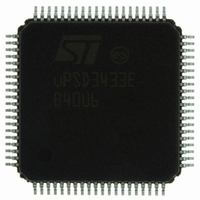
UPSD3433EB40U6 STMicroelectronics, UPSD3433EB40U6 Datasheet - Page 47

UPSD3433EB40U6
Manufacturer Part Number
UPSD3433EB40U6
Description
MCU 8BIT 8032 128KB FLASH 80TQFP
Manufacturer
STMicroelectronics
Series
µPSDr
Datasheet
1.UPSD3434EB40T6.pdf
(293 pages)
Specifications of UPSD3433EB40U6
Core Processor
8032
Core Size
8-Bit
Speed
40MHz
Connectivity
I²C, IrDA, SPI, UART/USART, USB
Peripherals
LVD, POR, PWM, WDT
Number Of I /o
46
Program Memory Size
160KB (160K x 8)
Program Memory Type
FLASH
Ram Size
8K x 8
Voltage - Supply (vcc/vdd)
3 V ~ 5.5 V
Data Converters
A/D 8x10b
Oscillator Type
Internal
Operating Temperature
-40°C ~ 85°C
Package / Case
80-TQFP, 80-VQFP
For Use With
497-5518 - EVAL BOARD RFID READER497-5046 - KIT TOOL FOR ST7/UPSD/STR7 MCU
Lead Free Status / RoHS Status
Lead free / RoHS Compliant
Eeprom Size
-
Other names
497-5660
Available stocks
Company
Part Number
Manufacturer
Quantity
Price
Company:
Part Number:
UPSD3433EB40U6
Manufacturer:
STMicroelectronics
Quantity:
10 000
- Current page: 47 of 293
- Download datasheet (5Mb)
uPSD34xx
11
11.1
Dual data pointers
XDATA is accessed by the External Direct addressing mode, which uses a 16-bit address
stored in the DPTR Register. Traditional 8032 architecture has only one DPTR Register.
This is a burden when transferring data between two XDATA locations because it requires
heavy use of the working registers to manipulate the source and destination pointers.
However, the uPSD34xx has two data pointers, one for storing a source address and the
other for storing a destination address. These pointers can be configured to automatically
increment or decrement after each data transfer, further reducing the burden on the 8032
and making this kind of data movement very efficient.
Data pointer control register, DPTC (85h)
By default, the DPTR Register of the uPSD34xx will behave no different than in a standard
8032 MCU. The DPSEL0 Bit of SFR register DPTC shown in
the two “background” data pointer registers (DPTR0 or DPTR1) will function as the
traditional DPTR Register at any given time. After reset, the DPSEL0 Bit is cleared, enabling
DPTR0 to function as the DPTR, and firmware may access DPTR0 by reading or writing the
traditional DPTR Register at SFR addresses 82h and 83h. When the DPSEL0 bit is set,
then the DPTR1 Register functions as DPTR, and firmware may now access DPTR1
through SFR registers at 82h and 83h. The pointer which is not selected by the DPSEL0 bit
remains in the background and is not accessible by the 8032. If the DPSEL0 bit is never set,
then the uPSD34xx will behave like a traditional 8032 having only one DPTR Register.
To further speed XDATA to XDATA transfers, the SFR bit, AT, may be set to automatically
toggle the two data pointers, DPTR0 and DPTR1, each time the standard DPTR Register is
accessed by a MOVX instruction. This eliminates the need for firmware to manually
manipulate the DPSEL0 bit between each data transfer.
Detailed description for the SFR register DPTC is shown in
Table 13.
Bit 7
5-1
Bit
–
7
6
0
DPTC: data pointer control register (SFR 85h, reset value 00h)
Symbol
DPSE0
Bit 6
AT
AT
–
–
Bit 5
R/W
R,W
R,W
–
–
–
Reserved
0 = Manually Select Data Pointer
1 = Auto Toggle between DPTR0 and DPTR1
Reserved
0 = DPTR0 Selected for use as DPTR
1 = DPTR1 Selected for use as DPTR
Bit 4
–
Bit 3
–
Definition
Table
Bit 2
Table
–
13.
13, selects which one of
Dual data pointers
Bit 1
–
DPSEL0
Bit 0
47/293
Related parts for UPSD3433EB40U6
Image
Part Number
Description
Manufacturer
Datasheet
Request
R

Part Number:
Description:
MCU 8BIT 8032 128KB FLASH 80TQFP
Manufacturer:
STMicroelectronics
Datasheet:

Part Number:
Description:
MCU 8BIT 8032 128KB FLASH 52TQFP
Manufacturer:
STMicroelectronics
Datasheet:

Part Number:
Description:
STMicroelectronics [RIPPLE-CARRY BINARY COUNTER/DIVIDERS]
Manufacturer:
STMicroelectronics
Datasheet:

Part Number:
Description:
STMicroelectronics [LIQUID-CRYSTAL DISPLAY DRIVERS]
Manufacturer:
STMicroelectronics
Datasheet:

Part Number:
Description:
BOARD EVAL FOR MEMS SENSORS
Manufacturer:
STMicroelectronics
Datasheet:

Part Number:
Description:
NPN TRANSISTOR POWER MODULE
Manufacturer:
STMicroelectronics
Datasheet:

Part Number:
Description:
TURBOSWITCH ULTRA-FAST HIGH VOLTAGE DIODE
Manufacturer:
STMicroelectronics
Datasheet:

Part Number:
Description:
Manufacturer:
STMicroelectronics
Datasheet:

Part Number:
Description:
DIODE / SCR MODULE
Manufacturer:
STMicroelectronics
Datasheet:

Part Number:
Description:
DIODE / SCR MODULE
Manufacturer:
STMicroelectronics
Datasheet:

Part Number:
Description:
Search -----> STE16N100
Manufacturer:
STMicroelectronics
Datasheet:

Part Number:
Description:
Search ---> STE53NA50
Manufacturer:
STMicroelectronics
Datasheet:


