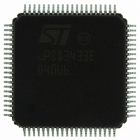
UPSD3433EB40U6 STMicroelectronics, UPSD3433EB40U6 Datasheet - Page 213

UPSD3433EB40U6
Manufacturer Part Number
UPSD3433EB40U6
Description
MCU 8BIT 8032 128KB FLASH 80TQFP
Manufacturer
STMicroelectronics
Series
µPSDr
Datasheet
1.UPSD3434EB40T6.pdf
(293 pages)
Specifications of UPSD3433EB40U6
Core Processor
8032
Core Size
8-Bit
Speed
40MHz
Connectivity
I²C, IrDA, SPI, UART/USART, USB
Peripherals
LVD, POR, PWM, WDT
Number Of I /o
46
Program Memory Size
160KB (160K x 8)
Program Memory Type
FLASH
Ram Size
8K x 8
Voltage - Supply (vcc/vdd)
3 V ~ 5.5 V
Data Converters
A/D 8x10b
Oscillator Type
Internal
Operating Temperature
-40°C ~ 85°C
Package / Case
80-TQFP, 80-VQFP
For Use With
497-5518 - EVAL BOARD RFID READER497-5046 - KIT TOOL FOR ST7/UPSD/STR7 MCU
Lead Free Status / RoHS Status
Lead free / RoHS Compliant
Eeprom Size
-
Other names
497-5660
Available stocks
Company
Part Number
Manufacturer
Quantity
Price
Company:
Part Number:
UPSD3433EB40U6
Manufacturer:
STMicroelectronics
Quantity:
10 000
- Current page: 213 of 293
- Download datasheet (5Mb)
uPSD34xx
Note:
28.5.25
The DPLD performs address decoding, and generates select signals for internal and
external components, such as memory, registers, and I/O ports. The DPLD can generate
External Chip-Select (ECS1-ECS2) signals on Port D.
The GPLD can be used for logic functions, such as loadable counters and shift registers,
state machines, encoding and decoding logic. These logic functions can be constructed
from a combination of 16 Output Macrocells (OMC), 20 Input Macrocells (IMC), and the
AND-OR Array.
Routing of the 16 OMCs outputs can be divided between pins on three Ports A, B, or C by
the OMC Allocator as shown in
routed to pins on Port A or Port B and are named MCELLAB0-MCELLAB7. The other eight
OMCs to be routed to pins on Port B or Port C and are named MCELLBC0-MCELLBC7.
This routing depends on the pin number assignments that are specified in PSDsoft Express
for “PLD Outputs” in the Pin Definition section. OMC outputs can also be routed internally
(not to pins) used as buried nodes to create shifters, counters, etc.
The AND-OR Array is used to form product terms. These product terms are configured from
the logic definitions entered in PSDsoft Express. A PLD Input Bus consisting of 69 signals is
connected to both PLDs. Input signals are shown in
compliment versions of each of these signals are available at inputs to each PLD.
The 8032 data bus, D0 - D7, does not route directly to PLD inputs. Instead, the 8032 data
bus has indirect access to the GPLD (not the DPLD) when the 8032 reads and writes the
OMC and IMC registers within csiop address space.
Turbo bit and PLDs
The PLDs can minimize power consumption by going to standby after ALL the PLD inputs
remain unchanged for an extended time (about 70ns). When the Turbo Bit is set to logic one
(Bit 3 of the csiop PMMR0 Register), Turbo mode is turned off and then this automatic
standby mode is achieved. Turning off Turbo mode increases propagation delays while
reducing power consumption. The default state of the Turbo Bit is logic zero, meaning Turbo
mode is on. Additionally, four bits are available in the csiop PMMR0 and PMMR2 Registers
to block the 8032 bus control signals (RD, WR, PSEN, ALE) from entering the PLDs. This
reduces power consumption and can be used only when these 8032 control signals are not
used in PLD logic equations. See
Figure 78 on page
Section 28.5.51: Power management on page
221. Eight of the 16 OMCs that can be
Table
111, both the true and
PSD module
241.
213/293
Related parts for UPSD3433EB40U6
Image
Part Number
Description
Manufacturer
Datasheet
Request
R

Part Number:
Description:
MCU 8BIT 8032 128KB FLASH 80TQFP
Manufacturer:
STMicroelectronics
Datasheet:

Part Number:
Description:
MCU 8BIT 8032 128KB FLASH 52TQFP
Manufacturer:
STMicroelectronics
Datasheet:

Part Number:
Description:
STMicroelectronics [RIPPLE-CARRY BINARY COUNTER/DIVIDERS]
Manufacturer:
STMicroelectronics
Datasheet:

Part Number:
Description:
STMicroelectronics [LIQUID-CRYSTAL DISPLAY DRIVERS]
Manufacturer:
STMicroelectronics
Datasheet:

Part Number:
Description:
BOARD EVAL FOR MEMS SENSORS
Manufacturer:
STMicroelectronics
Datasheet:

Part Number:
Description:
NPN TRANSISTOR POWER MODULE
Manufacturer:
STMicroelectronics
Datasheet:

Part Number:
Description:
TURBOSWITCH ULTRA-FAST HIGH VOLTAGE DIODE
Manufacturer:
STMicroelectronics
Datasheet:

Part Number:
Description:
Manufacturer:
STMicroelectronics
Datasheet:

Part Number:
Description:
DIODE / SCR MODULE
Manufacturer:
STMicroelectronics
Datasheet:

Part Number:
Description:
DIODE / SCR MODULE
Manufacturer:
STMicroelectronics
Datasheet:

Part Number:
Description:
Search -----> STE16N100
Manufacturer:
STMicroelectronics
Datasheet:

Part Number:
Description:
Search ---> STE53NA50
Manufacturer:
STMicroelectronics
Datasheet:


