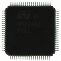
UPSD3433EB40U6 STMicroelectronics, UPSD3433EB40U6 Datasheet - Page 202

UPSD3433EB40U6
Manufacturer Part Number
UPSD3433EB40U6
Description
MCU 8BIT 8032 128KB FLASH 80TQFP
Manufacturer
STMicroelectronics
Series
µPSDr
Datasheet
1.UPSD3434EB40T6.pdf
(293 pages)
Specifications of UPSD3433EB40U6
Core Processor
8032
Core Size
8-Bit
Speed
40MHz
Connectivity
I²C, IrDA, SPI, UART/USART, USB
Peripherals
LVD, POR, PWM, WDT
Number Of I /o
46
Program Memory Size
160KB (160K x 8)
Program Memory Type
FLASH
Ram Size
8K x 8
Voltage - Supply (vcc/vdd)
3 V ~ 5.5 V
Data Converters
A/D 8x10b
Oscillator Type
Internal
Operating Temperature
-40°C ~ 85°C
Package / Case
80-TQFP, 80-VQFP
For Use With
497-5518 - EVAL BOARD RFID READER497-5046 - KIT TOOL FOR ST7/UPSD/STR7 MCU
Lead Free Status / RoHS Status
Lead free / RoHS Compliant
Eeprom Size
-
Other names
497-5660
Available stocks
Company
Part Number
Manufacturer
Quantity
Price
Company:
Part Number:
UPSD3433EB40U6
Manufacturer:
STMicroelectronics
Quantity:
10 000
- Current page: 202 of 293
- Download datasheet (5Mb)
PSD module
28.5.2
202/293
Important note: The 8032 may not read and execute code from the same Flash memory
array for which it is directing an instruction sequence. Or more simply stated, the 8032 may
not read code from the same Flash array that is writing or erasing. Instead, the 8032 must
execute code from an alternate memory (like SRAM or a different Flash array) while sending
instruction sequences to a given Flash array. Since the two Flash memory arrays inside the
PSD Module device are completely independent, the 8032 may read code from one array
while sending instructions to the other. It is possible, however, to suspend a sector erase
operation in one particular Flash array in order to access a different sector within that same
Flash array, then resume the erase later.
After a Flash memory array is programmed or erased it will go to “Read Array” mode, then
the 8032 can read from Flash memory just as it would read from any ROM or SRAM device.
Flash memory instruction sequences
An instruction sequence consists of a sequence of specific byte WRITE and byte READ
operations. Each byte written to either Flash memory array on the PSD Module is received
by a state machine inside the Flash array and sequentially decoded to execute an
embedded algorithm. The algorithm is executed when the correct number of bytes are
properly received and the time between two consecutive bytes is shorter than the time-out
period of 80µs. Some instruction sequences are structured to include READ operations
after the initial WRITE operations.
An instruction sequence must be followed exactly. Any invalid combination of instruction
bytes or time-out between two consecutive bytes while addressing Flash memory resets the
PSD Module Flash logic into Read Array mode (where Flash memory is read like a ROM
device). The Flash memories support instruction sequences summarized in
page
●
●
●
●
●
The first two bytes of an instruction sequence are 8032 bus WRITE operations to “unlock”
the Flash array, followed by writing a command byte. The bus operations consist of writing
the data AAh to address X555h during the first bus cycle and data 55h to address XAAAh
during the second bus cycle. 8032 address signals A12-A15 are “Don’t care” during the
instruction sequence during WRITE cycles. However, the appropriate sector select signal
(FSx or CSBOOTx) from the DPLD must be active during the entire instruction sequence to
complete the entire 8032 address (this includes the page number when memory paging is
used). Ignoring A12-A15 means the user has more flexibility in memory mapping. For
example, in many traditional Flash memories, instruction sequences must be written to
addresses AAAAh and 5555h, not XAAAh and X555h like supported on the PSD Module.
When the user has to write to AAAAh and 5555h, the memory mapping options are limited.
The Main Flash and Secondary Flash memories each have the same instruction set shown
in
receive and execute the instructions.
Table 107 on page
Program a Byte
Unlock Sequence Bypass
Erase memory by array or by sector
Suspend or resume a sector erase
Reset to Read Array mode
203.
203, but the sector select signals determine which memory array will
Table 107 on
uPSD34xx
Related parts for UPSD3433EB40U6
Image
Part Number
Description
Manufacturer
Datasheet
Request
R

Part Number:
Description:
MCU 8BIT 8032 128KB FLASH 80TQFP
Manufacturer:
STMicroelectronics
Datasheet:

Part Number:
Description:
MCU 8BIT 8032 128KB FLASH 52TQFP
Manufacturer:
STMicroelectronics
Datasheet:

Part Number:
Description:
STMicroelectronics [RIPPLE-CARRY BINARY COUNTER/DIVIDERS]
Manufacturer:
STMicroelectronics
Datasheet:

Part Number:
Description:
STMicroelectronics [LIQUID-CRYSTAL DISPLAY DRIVERS]
Manufacturer:
STMicroelectronics
Datasheet:

Part Number:
Description:
BOARD EVAL FOR MEMS SENSORS
Manufacturer:
STMicroelectronics
Datasheet:

Part Number:
Description:
NPN TRANSISTOR POWER MODULE
Manufacturer:
STMicroelectronics
Datasheet:

Part Number:
Description:
TURBOSWITCH ULTRA-FAST HIGH VOLTAGE DIODE
Manufacturer:
STMicroelectronics
Datasheet:

Part Number:
Description:
Manufacturer:
STMicroelectronics
Datasheet:

Part Number:
Description:
DIODE / SCR MODULE
Manufacturer:
STMicroelectronics
Datasheet:

Part Number:
Description:
DIODE / SCR MODULE
Manufacturer:
STMicroelectronics
Datasheet:

Part Number:
Description:
Search -----> STE16N100
Manufacturer:
STMicroelectronics
Datasheet:

Part Number:
Description:
Search ---> STE53NA50
Manufacturer:
STMicroelectronics
Datasheet:


