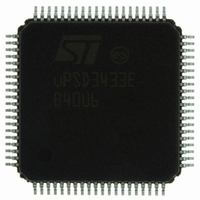
UPSD3433EB40U6 STMicroelectronics, UPSD3433EB40U6 Datasheet - Page 29

UPSD3433EB40U6
Manufacturer Part Number
UPSD3433EB40U6
Description
MCU 8BIT 8032 128KB FLASH 80TQFP
Manufacturer
STMicroelectronics
Series
µPSDr
Datasheet
1.UPSD3434EB40T6.pdf
(293 pages)
Specifications of UPSD3433EB40U6
Core Processor
8032
Core Size
8-Bit
Speed
40MHz
Connectivity
I²C, IrDA, SPI, UART/USART, USB
Peripherals
LVD, POR, PWM, WDT
Number Of I /o
46
Program Memory Size
160KB (160K x 8)
Program Memory Type
FLASH
Ram Size
8K x 8
Voltage - Supply (vcc/vdd)
3 V ~ 5.5 V
Data Converters
A/D 8x10b
Oscillator Type
Internal
Operating Temperature
-40°C ~ 85°C
Package / Case
80-TQFP, 80-VQFP
For Use With
497-5518 - EVAL BOARD RFID READER497-5046 - KIT TOOL FOR ST7/UPSD/STR7 MCU
Lead Free Status / RoHS Status
Lead free / RoHS Compliant
Eeprom Size
-
Other names
497-5660
Available stocks
Company
Part Number
Manufacturer
Quantity
Price
Company:
Part Number:
UPSD3433EB40U6
Manufacturer:
STMicroelectronics
Quantity:
10 000
- Current page: 29 of 293
- Download datasheet (5Mb)
uPSD34xx
7.5
7.6
7.7
7.7.1
7.7.2
7.7.3
7.7.4
7.7.5
the B Register to hold 16-bit operands. The ACC is referred to as “A” in the MCU instruction
set.
B register (B)
The B Register is a general purpose 8-bit register for temporary data storage and also used
as a 16-bit register when concatenated with the ACC Register for use with MUL and DIV
instructions.
General purpose registers (R0 - R7)
There are four banks of eight general purpose 8-bit registers (R0 - R7), but only one bank of
eight registers is active at any given time depending on the setting in the PSW word
(described next). R0 - R7 are generally used to assist in manipulating values and moving
data from one memory location to another. These register banks physically reside in the first
32 locations of 8032 internal DATA SRAM, starting at address 00h. At reset, only the first
bank of eight registers is active (addresses 00h to 07h), and the stack begins at address
08h.
Program status word (PSW)
The PSW is an 8-bit register which stores several important bits, or flags, that are set and
cleared by many 8032 instructions, reflecting the current state of the MCU core.
on page 30
Carry flag (CY)
This flag is set when the last arithmetic operation that was executed results in a carry
(addition) or borrow (subtraction). It is cleared by all other arithmetic operations. The CY flag
is also affected by Shift and Rotate Instructions.
Auxiliary carry flag (AC)
This flag is set when the last arithmetic operation that was executed results in a carry into
(addition) or borrow from (subtraction) the high-order nibble. It is cleared by all other
arithmetic operations.
General purpose flag (F0)
This is a bit-addressable, general-purpose flag for use under software control.
Register bank select flags (RS1, RS0)
These bits select which bank of eight registers is used during R0 - R7 register accesses
(see
Overflow flag (OV)
The OV flag is set when: an ADD, ADDC, or SUBB instruction causes a sign change; a MUL
instruction results in an overflow (result greater than 255); a DIV instruction causes a divide-
Table
4)
shows the individual flags.
8032 MCU registers
Figure 12
29/293
Related parts for UPSD3433EB40U6
Image
Part Number
Description
Manufacturer
Datasheet
Request
R

Part Number:
Description:
MCU 8BIT 8032 128KB FLASH 80TQFP
Manufacturer:
STMicroelectronics
Datasheet:

Part Number:
Description:
MCU 8BIT 8032 128KB FLASH 52TQFP
Manufacturer:
STMicroelectronics
Datasheet:

Part Number:
Description:
STMicroelectronics [RIPPLE-CARRY BINARY COUNTER/DIVIDERS]
Manufacturer:
STMicroelectronics
Datasheet:

Part Number:
Description:
STMicroelectronics [LIQUID-CRYSTAL DISPLAY DRIVERS]
Manufacturer:
STMicroelectronics
Datasheet:

Part Number:
Description:
BOARD EVAL FOR MEMS SENSORS
Manufacturer:
STMicroelectronics
Datasheet:

Part Number:
Description:
NPN TRANSISTOR POWER MODULE
Manufacturer:
STMicroelectronics
Datasheet:

Part Number:
Description:
TURBOSWITCH ULTRA-FAST HIGH VOLTAGE DIODE
Manufacturer:
STMicroelectronics
Datasheet:

Part Number:
Description:
Manufacturer:
STMicroelectronics
Datasheet:

Part Number:
Description:
DIODE / SCR MODULE
Manufacturer:
STMicroelectronics
Datasheet:

Part Number:
Description:
DIODE / SCR MODULE
Manufacturer:
STMicroelectronics
Datasheet:

Part Number:
Description:
Search -----> STE16N100
Manufacturer:
STMicroelectronics
Datasheet:

Part Number:
Description:
Search ---> STE53NA50
Manufacturer:
STMicroelectronics
Datasheet:


