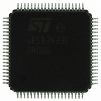
UPSD3433EB40U6 STMicroelectronics, UPSD3433EB40U6 Datasheet - Page 255

UPSD3433EB40U6
Manufacturer Part Number
UPSD3433EB40U6
Description
MCU 8BIT 8032 128KB FLASH 80TQFP
Manufacturer
STMicroelectronics
Series
µPSDr
Datasheet
1.UPSD3434EB40T6.pdf
(293 pages)
Specifications of UPSD3433EB40U6
Core Processor
8032
Core Size
8-Bit
Speed
40MHz
Connectivity
I²C, IrDA, SPI, UART/USART, USB
Peripherals
LVD, POR, PWM, WDT
Number Of I /o
46
Program Memory Size
160KB (160K x 8)
Program Memory Type
FLASH
Ram Size
8K x 8
Voltage - Supply (vcc/vdd)
3 V ~ 5.5 V
Data Converters
A/D 8x10b
Oscillator Type
Internal
Operating Temperature
-40°C ~ 85°C
Package / Case
80-TQFP, 80-VQFP
For Use With
497-5518 - EVAL BOARD RFID READER497-5046 - KIT TOOL FOR ST7/UPSD/STR7 MCU
Lead Free Status / RoHS Status
Lead free / RoHS Compliant
Eeprom Size
-
Other names
497-5660
Available stocks
Company
Part Number
Manufacturer
Quantity
Price
Company:
Part Number:
UPSD3433EB40U6
Manufacturer:
STMicroelectronics
Quantity:
10 000
- Current page: 255 of 293
- Download datasheet (5Mb)
uPSD34xx
Note:
Note:
2
3
1
TSTAT and TERR are functional only when JTAG ISP operations are occurring, which
means they are non-functional during JTAG debugging of the 8032 on the MCU Module.
Programming times vary depending on the number of locations to be programmed and the
JTAG programming equipment, but typical JTAG ISP programming times are 10 to 25
seconds using 6-pin JTAG. The signals TSTAT and TERR are not included in the IEEE
1149.1 specification.
Figure 93 on page 255
program/test tool using 6-pin JTAG. It is required to connect the RST output signal from the
JTAG program/test equipment to the RESET_IN input on the uPSD34xx. The RST signal is
driven by the equipment with an Open Drain driver, allowing other sources (like a push
button) to drive RESET_IN without conflict.
The recommended pull-up resistors and decoupling capacitor are illustrated in
Figure 93. Recommended 6-pin JTAG connections
For 5V uPSD34xx devices, pull-up resistors and V
connected to 5V system V
For 3.3V uPSD34xx devices, pull-up resistors and V
connected to 3.3V system V
This signal is driven by an Open-Drain output in the JTAG equipment, allowing more than
one source to activate RESET_IN.
uPSD34xx
SRAM STBY or I/O - PC2
CIRCUIT
BOARD
GENERAL I/O - PC7
TSTAT - PC3
TERR - PC4
TDO - PC6
TMS - PC0
TCK - PC1
TDI - PC5
RESETIN
DEBUG
shows recommended connections on a circuit board to a JTAG
DD
CC
.
.
100k
TEST POINT
OPTIONAL
GENERAL I/O
SIGNALS
RESET SOURCE
PUSH BUTTON
or ANY OTHER
CC
100k typical
CC
pin on the JTAG connector should be
10k
pin on the JTAG connector should be
0.01
µF
CONN.
JTAG
TMS
V
TCK
TERR
TDI
TDO
GND
TSTAT
RST
CC
(1,2)
(3)
PSD module
Figure
JTAG
Programming
or Test
Equipment
Connects Here
AI10458
255/293
93.
Related parts for UPSD3433EB40U6
Image
Part Number
Description
Manufacturer
Datasheet
Request
R

Part Number:
Description:
MCU 8BIT 8032 128KB FLASH 80TQFP
Manufacturer:
STMicroelectronics
Datasheet:

Part Number:
Description:
MCU 8BIT 8032 128KB FLASH 52TQFP
Manufacturer:
STMicroelectronics
Datasheet:

Part Number:
Description:
STMicroelectronics [RIPPLE-CARRY BINARY COUNTER/DIVIDERS]
Manufacturer:
STMicroelectronics
Datasheet:

Part Number:
Description:
STMicroelectronics [LIQUID-CRYSTAL DISPLAY DRIVERS]
Manufacturer:
STMicroelectronics
Datasheet:

Part Number:
Description:
BOARD EVAL FOR MEMS SENSORS
Manufacturer:
STMicroelectronics
Datasheet:

Part Number:
Description:
NPN TRANSISTOR POWER MODULE
Manufacturer:
STMicroelectronics
Datasheet:

Part Number:
Description:
TURBOSWITCH ULTRA-FAST HIGH VOLTAGE DIODE
Manufacturer:
STMicroelectronics
Datasheet:

Part Number:
Description:
Manufacturer:
STMicroelectronics
Datasheet:

Part Number:
Description:
DIODE / SCR MODULE
Manufacturer:
STMicroelectronics
Datasheet:

Part Number:
Description:
DIODE / SCR MODULE
Manufacturer:
STMicroelectronics
Datasheet:

Part Number:
Description:
Search -----> STE16N100
Manufacturer:
STMicroelectronics
Datasheet:

Part Number:
Description:
Search ---> STE53NA50
Manufacturer:
STMicroelectronics
Datasheet:


