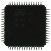
UPSD3433EB40U6 STMicroelectronics, UPSD3433EB40U6 Datasheet - Page 203

UPSD3433EB40U6
Manufacturer Part Number
UPSD3433EB40U6
Description
MCU 8BIT 8032 128KB FLASH 80TQFP
Manufacturer
STMicroelectronics
Series
µPSDr
Datasheet
1.UPSD3434EB40T6.pdf
(293 pages)
Specifications of UPSD3433EB40U6
Core Processor
8032
Core Size
8-Bit
Speed
40MHz
Connectivity
I²C, IrDA, SPI, UART/USART, USB
Peripherals
LVD, POR, PWM, WDT
Number Of I /o
46
Program Memory Size
160KB (160K x 8)
Program Memory Type
FLASH
Ram Size
8K x 8
Voltage - Supply (vcc/vdd)
3 V ~ 5.5 V
Data Converters
A/D 8x10b
Oscillator Type
Internal
Operating Temperature
-40°C ~ 85°C
Package / Case
80-TQFP, 80-VQFP
For Use With
497-5518 - EVAL BOARD RFID READER497-5046 - KIT TOOL FOR ST7/UPSD/STR7 MCU
Lead Free Status / RoHS Status
Lead free / RoHS Compliant
Eeprom Size
-
Other names
497-5660
Available stocks
Company
Part Number
Manufacturer
Quantity
Price
Company:
Part Number:
UPSD3433EB40U6
Manufacturer:
STMicroelectronics
Quantity:
10 000
- Current page: 203 of 293
- Download datasheet (5Mb)
uPSD34xx
Note:
1
2
Table 107. Flash memory instruction sequences
All values are in hexadecimal, X = Don’t care
8032 addresses A12 through A15 are “Don’t care” during the instruction sequence
decoding. Only address bits A0-A11 are used during decoding of Flash memory instruction
Read
Memory
Contents
(Read
Array
mode)
Program
(write) a
Byte to
Flash
Memory
Bypass
Unlock
Program a
Byte to
Flash
Memory
with
Bypassed
Unlock
Reset
Bypass
Unlock
Flash Bulk
Erase
Flash
Sector
Erase
Suspend
Sector
Erase
Resume
Sector
Erase
Reset
Flash
Instr.
Seq.
(3)
Read byte
from any valid
Flash
memory addr
Write AAh to
X555h
(unlock)
Write AAh to
X555h
(unlock)
Write A0h to
XXXXh
(command)
Write 90h to
XXXXh
(command)
Write AAh to
X555h
(unlock)
Write AAh to
X555h
(unlock)
Write B0h to
address that
activates FSx
or CSBOOTx
where erase
is in progress
(command)
Write 30h to
address that
activates FSx
or CSBOOTx
where
desired to
resume erase
(command)
Write F0h to
address that
activates FSx
or CSBOOTx
in desired
array.
(command)
Cycle 1
Bus
Write 55h
to XAAAh
(unlock)
Write 55h
to XAAAh
(unlock)
Write data
byte to
address
Write 00h
to XXXXh
(command)
Write 55h
to XAAAh
(unlock)
Write 55h
to XAAAh
(unlock)
Cycle 2
Bus
Write A0h
to X555h
(command)
Write 20h
to X555h
(command)
Write 80h
to X555h
(command)
Write 80h
to X555h
(command)
Cycle 3
Bus
Write data
byte to
address
Write AAh
to X555h
(unlock)
Write AAh
to X555h
(unlock)
Cycle 4
Bus
Write 55h
to XAAAh
(unlock)
Write 55h
to XAAAh
(unlock)
Cycle 5
Bus
(1,2)
Write 10h to
X555h
(command)
Write 30h to
desired
Sector
(command)
Cycle 6
Bus
Write 30h to
another
Sector
(command)
Cycle 7
Bus
PSD module
Flash memory.
Read memory
Programming
sequence on
sequence on
sequence on
contents. on
on page 205
Flash sector
sector erase
on page 210
sector erase
on page 211
on page 211
Reset Flash
Flash bulk
Bypassed
Bypassed
Bypassed
page 204
page 209
page 209
page 209
page 209
page 210
Suspend
erase on
erase on
Resume
unlock
unlock
unlock
Link
203/293
Related parts for UPSD3433EB40U6
Image
Part Number
Description
Manufacturer
Datasheet
Request
R

Part Number:
Description:
MCU 8BIT 8032 128KB FLASH 80TQFP
Manufacturer:
STMicroelectronics
Datasheet:

Part Number:
Description:
MCU 8BIT 8032 128KB FLASH 52TQFP
Manufacturer:
STMicroelectronics
Datasheet:

Part Number:
Description:
STMicroelectronics [RIPPLE-CARRY BINARY COUNTER/DIVIDERS]
Manufacturer:
STMicroelectronics
Datasheet:

Part Number:
Description:
STMicroelectronics [LIQUID-CRYSTAL DISPLAY DRIVERS]
Manufacturer:
STMicroelectronics
Datasheet:

Part Number:
Description:
BOARD EVAL FOR MEMS SENSORS
Manufacturer:
STMicroelectronics
Datasheet:

Part Number:
Description:
NPN TRANSISTOR POWER MODULE
Manufacturer:
STMicroelectronics
Datasheet:

Part Number:
Description:
TURBOSWITCH ULTRA-FAST HIGH VOLTAGE DIODE
Manufacturer:
STMicroelectronics
Datasheet:

Part Number:
Description:
Manufacturer:
STMicroelectronics
Datasheet:

Part Number:
Description:
DIODE / SCR MODULE
Manufacturer:
STMicroelectronics
Datasheet:

Part Number:
Description:
DIODE / SCR MODULE
Manufacturer:
STMicroelectronics
Datasheet:

Part Number:
Description:
Search -----> STE16N100
Manufacturer:
STMicroelectronics
Datasheet:

Part Number:
Description:
Search ---> STE53NA50
Manufacturer:
STMicroelectronics
Datasheet:


