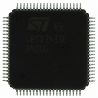
UPSD3433EB40U6 STMicroelectronics, UPSD3433EB40U6 Datasheet - Page 70

UPSD3433EB40U6
Manufacturer Part Number
UPSD3433EB40U6
Description
MCU 8BIT 8032 128KB FLASH 80TQFP
Manufacturer
STMicroelectronics
Series
µPSDr
Datasheet
1.UPSD3434EB40T6.pdf
(293 pages)
Specifications of UPSD3433EB40U6
Core Processor
8032
Core Size
8-Bit
Speed
40MHz
Connectivity
I²C, IrDA, SPI, UART/USART, USB
Peripherals
LVD, POR, PWM, WDT
Number Of I /o
46
Program Memory Size
160KB (160K x 8)
Program Memory Type
FLASH
Ram Size
8K x 8
Voltage - Supply (vcc/vdd)
3 V ~ 5.5 V
Data Converters
A/D 8x10b
Oscillator Type
Internal
Operating Temperature
-40°C ~ 85°C
Package / Case
80-TQFP, 80-VQFP
For Use With
497-5518 - EVAL BOARD RFID READER497-5046 - KIT TOOL FOR ST7/UPSD/STR7 MCU
Lead Free Status / RoHS Status
Lead free / RoHS Compliant
Eeprom Size
-
Other names
497-5660
Available stocks
Company
Part Number
Manufacturer
Quantity
Price
Company:
Part Number:
UPSD3433EB40U6
Manufacturer:
STMicroelectronics
Quantity:
10 000
- Current page: 70 of 293
- Download datasheet (5Mb)
I/O ports of mcu module
17.1.1
17.1.2
17.1.3
70/293
GPIO function
Ports in GPIO mode operate as quasi-bidirectional pins, consistent with standard 8051
architecture. GPIO pins are individually controlled by three SFRs:
●
●
●
These SFRs can be accessed using the Bit Addressing mode, an efficient way to control
individual port pins.
GPIO output
Simply stated, when a logic '0' is written to a bit in any of these port SFRs while in GPIO
mode, the corresponding port pin will enable a low-side driver, which pulls the pin to ground,
and at the same time releases the high-side driver and pull-ups, resulting in a logic '0'
output. When a logic '1' is written to the SFR, the low-side driver is released, the high-side
driver is enabled for just one MCU_CLK period to rapidly make the 0-to1 transition on the
pin, while weak active pull-ups (total ~150KΩ) to V
consistent with standard 8051 architecture. The high side driver is momentarily enabled only
for 0-to-1 transitions, which is implemented with the delay function at the latch output as
pictured in
the high-side driver is disabled, the two weak pull-ups remain enabled resulting in a logic '1'
output at the pin, sourcing I
resistor can be added if additional source current is needed while outputting a logic '1.'
GPIO input
To use a GPIO port pin as an input, the low-side driver to ground must be disabled, or else
the true logic level being driven on the pin by an external device will be masked (always
reads logic '0'). So to make a port pin “input ready”, the corresponding bit in the SFR must
have been set to a logic '1' prior to reading that SFR bit as an input. A reset condition forces
SFRs P1, P3, and P4 to FFh, thus all three ports are input ready after reset.
When a pin is used as an input, the stronger pull-up “A” maintains a solid logic '1' until an
external device drives the input pin low. At this time, pull-up “A” is automatically disabled,
and only pull-up “B” will source the external device I
architecture.
GPIO Bi-Directional. It is possible to operate individual port pins in bi-directional mode. For
an output, firmware would simply write the corresponding SFR bit to logic '1' or '0' as
needed. But before using the pin as an input, firmware must first ensure that a logic '1' was
the last value written to the corresponding SFR bit prior to reading that SFR bit as an input.
GPIO Current Capability. A GPIO pin on Port 4 can sink twice as much current than a pin
on either Port 1 or Port 3 when the low-side driver is outputting a logic '0' (I
specifications at the end of this document for full details.
Reading Port Pin vs. Reading Port Latch. When firmware reads the GPIO ports,
sometimes the actual port pin is sampled in hardware, and sometimes the port SFR latch is
read and not the actual pin, depending on the type of MCU instruction used. These two data
paths are shown in
read (and not the pins) only when the read is part of a read-modify-write instruction and the
write destination is a bit or bits in a port SFR. These instructions are: ANL, ORL, XRL, JBC,
SFR, P1
SFR, P3
SFR, P4
Figure 17 on page
(Table 27 on page
(Table 28 on page
(Table 29 on page
Figure 17 on page 71
OH
71,
uA to an external device. Optionally, an external pull-up
73)
73)
74)
Figure 18 on page
through
Figure 19 on page
CC
IH
72, and
are enabled. This structure is
uA, consistent with standard 8051
Figure 19 on page
72. SFR latches are
OL
). See the DC
72. After
uPSD34xx
Related parts for UPSD3433EB40U6
Image
Part Number
Description
Manufacturer
Datasheet
Request
R

Part Number:
Description:
MCU 8BIT 8032 128KB FLASH 80TQFP
Manufacturer:
STMicroelectronics
Datasheet:

Part Number:
Description:
MCU 8BIT 8032 128KB FLASH 52TQFP
Manufacturer:
STMicroelectronics
Datasheet:

Part Number:
Description:
STMicroelectronics [RIPPLE-CARRY BINARY COUNTER/DIVIDERS]
Manufacturer:
STMicroelectronics
Datasheet:

Part Number:
Description:
STMicroelectronics [LIQUID-CRYSTAL DISPLAY DRIVERS]
Manufacturer:
STMicroelectronics
Datasheet:

Part Number:
Description:
BOARD EVAL FOR MEMS SENSORS
Manufacturer:
STMicroelectronics
Datasheet:

Part Number:
Description:
NPN TRANSISTOR POWER MODULE
Manufacturer:
STMicroelectronics
Datasheet:

Part Number:
Description:
TURBOSWITCH ULTRA-FAST HIGH VOLTAGE DIODE
Manufacturer:
STMicroelectronics
Datasheet:

Part Number:
Description:
Manufacturer:
STMicroelectronics
Datasheet:

Part Number:
Description:
DIODE / SCR MODULE
Manufacturer:
STMicroelectronics
Datasheet:

Part Number:
Description:
DIODE / SCR MODULE
Manufacturer:
STMicroelectronics
Datasheet:

Part Number:
Description:
Search -----> STE16N100
Manufacturer:
STMicroelectronics
Datasheet:

Part Number:
Description:
Search ---> STE53NA50
Manufacturer:
STMicroelectronics
Datasheet:


