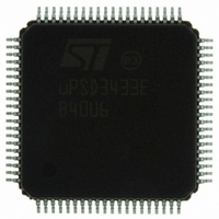
UPSD3433EB40U6 STMicroelectronics, UPSD3433EB40U6 Datasheet - Page 223

UPSD3433EB40U6
Manufacturer Part Number
UPSD3433EB40U6
Description
MCU 8BIT 8032 128KB FLASH 80TQFP
Manufacturer
STMicroelectronics
Series
µPSDr
Datasheet
1.UPSD3434EB40T6.pdf
(293 pages)
Specifications of UPSD3433EB40U6
Core Processor
8032
Core Size
8-Bit
Speed
40MHz
Connectivity
I²C, IrDA, SPI, UART/USART, USB
Peripherals
LVD, POR, PWM, WDT
Number Of I /o
46
Program Memory Size
160KB (160K x 8)
Program Memory Type
FLASH
Ram Size
8K x 8
Voltage - Supply (vcc/vdd)
3 V ~ 5.5 V
Data Converters
A/D 8x10b
Oscillator Type
Internal
Operating Temperature
-40°C ~ 85°C
Package / Case
80-TQFP, 80-VQFP
For Use With
497-5518 - EVAL BOARD RFID READER497-5046 - KIT TOOL FOR ST7/UPSD/STR7 MCU
Lead Free Status / RoHS Status
Lead free / RoHS Compliant
Eeprom Size
-
Other names
497-5660
Available stocks
Company
Part Number
Manufacturer
Quantity
Price
Company:
Part Number:
UPSD3433EB40U6
Manufacturer:
STMicroelectronics
Quantity:
10 000
- Current page: 223 of 293
- Download datasheet (5Mb)
uPSD34xx
28.5.32
Note:
Note:
28.5.33
1
2
1
2
OMC mask registers
There is one OMC Mask Register for each of the two groups of eight OMCs shown in
Table 115
individual OMCs. The default value for the mask registers is 00h, which allows loading of all
OMCs. When a given bit in a mask register is set to a '1,' the 8032 is blocked from writing to
the associated OMC flip-flop. For example, suppose that only four of eight OMCs
(MCELLAB0-3) are being used for a state machine. The user may not want the 8032 to write
to all the OMCs in MCELLAB because it would overwrite the state machine registers.
Therefore, the user would want to load the mask register for MCELLAB with the value 0Fh
before writing OMCs.
Table 115. Output macrocell MCELLAB mask register (address = csiop + offset 22h)
Default is 00h after any reset condition
1 = block writing to individual macrocell, 0 = allow writing to individual macrocell
Table 116. Output macrocell MCELLBC mask register (address = csiop + offset 23h)
Default is 00h after any reset condition
1 = block writing to individual macrocell, 0 = allow writing to individual macrocell
Input macrocells
The GPLD has 20 IMCs, one for each pin on Port A (80-pin device only), one for each pin on
Port B, and for the four pins on Port C that are not JTAG pins. The architecture of one
individual IMC is shown in
they can strobe a signal coming in from a port pin as a latch (gated), or as a register
(clocked), or the IMC can pass the signal without strobing, all prior to driving the signal onto
the PLD input bus. Strobing is useful for sampling and debouncing inputs (keypad inputs,
etc.) before entering the PLD AND-OR arrays. The outputs of IMCs can be read by the 8032
asynchronously when the 8032 reads the csiop registers shown in
and
different methods, one method is by reading IMCs as described here, the other method is
using MCU I/O mode described in a later section.
The optional IMC clocking or gating signal used to strobe pin inputs is driven by a product
term from the AND-OR array. There is one clocking or gating product term available for each
group of four IMCs. Port inputs 0-3 are controlled by one product term and 4-7 by another.
To specify in PSDsoft Express the method in which a signal will be strobed as it enters an
IMC for a given input pin on Port A, B, or C, just specify “PT Clocked Register” to use a rising
edge to clock the incoming signal, or specify “PT Clock Latch” to use an active high gate
signal to latch the incoming signal. Then define an equation for the IMC clock (.ld) or the
IMC gate (.le) signal in the “I/O Equations” section.
MCELLAB7
MCELLBC7
Bit 7
Bit 7
Mask
Mask
Table 119 on page
and
MCELLAB6
MCELLBC6
Table
Bit 6
Bit 6
Mask
Mask
116. The OMC mask registers are used to block loading of data to
224. It is possible to read a PSD Module port pin using one of two
MCELLAB5
MCELLBC5
Bit 5
Bit 5
Mask
Mask
Figure 79 on page
MCELLAB4
MCELLBC4
Bit 4
Bit 4
Mask
Mask
224. IMCs are individually configurable, and
MCELLAB3
MCELLBC3
Bit 3
Bit 3
Mask
Mask
MCELLAB2
MCELLBC2
Bit 2
Bit 2
Mask
Mask
Table
MCELLAB1
MCELLBC1
Bit 1
Bit 1
Mask
Mask
117,
Table
PSD module
MCELLAB0
MCELLBC0
Bit 0
Bit 0
118,
Mask
Mask
223/293
Related parts for UPSD3433EB40U6
Image
Part Number
Description
Manufacturer
Datasheet
Request
R

Part Number:
Description:
MCU 8BIT 8032 128KB FLASH 80TQFP
Manufacturer:
STMicroelectronics
Datasheet:

Part Number:
Description:
MCU 8BIT 8032 128KB FLASH 52TQFP
Manufacturer:
STMicroelectronics
Datasheet:

Part Number:
Description:
STMicroelectronics [RIPPLE-CARRY BINARY COUNTER/DIVIDERS]
Manufacturer:
STMicroelectronics
Datasheet:

Part Number:
Description:
STMicroelectronics [LIQUID-CRYSTAL DISPLAY DRIVERS]
Manufacturer:
STMicroelectronics
Datasheet:

Part Number:
Description:
BOARD EVAL FOR MEMS SENSORS
Manufacturer:
STMicroelectronics
Datasheet:

Part Number:
Description:
NPN TRANSISTOR POWER MODULE
Manufacturer:
STMicroelectronics
Datasheet:

Part Number:
Description:
TURBOSWITCH ULTRA-FAST HIGH VOLTAGE DIODE
Manufacturer:
STMicroelectronics
Datasheet:

Part Number:
Description:
Manufacturer:
STMicroelectronics
Datasheet:

Part Number:
Description:
DIODE / SCR MODULE
Manufacturer:
STMicroelectronics
Datasheet:

Part Number:
Description:
DIODE / SCR MODULE
Manufacturer:
STMicroelectronics
Datasheet:

Part Number:
Description:
Search -----> STE16N100
Manufacturer:
STMicroelectronics
Datasheet:

Part Number:
Description:
Search ---> STE53NA50
Manufacturer:
STMicroelectronics
Datasheet:


