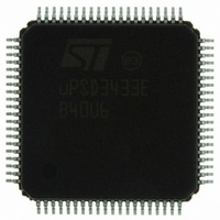
UPSD3433EB40U6 STMicroelectronics, UPSD3433EB40U6 Datasheet - Page 251

UPSD3433EB40U6
Manufacturer Part Number
UPSD3433EB40U6
Description
MCU 8BIT 8032 128KB FLASH 80TQFP
Manufacturer
STMicroelectronics
Series
µPSDr
Datasheet
1.UPSD3434EB40T6.pdf
(293 pages)
Specifications of UPSD3433EB40U6
Core Processor
8032
Core Size
8-Bit
Speed
40MHz
Connectivity
I²C, IrDA, SPI, UART/USART, USB
Peripherals
LVD, POR, PWM, WDT
Number Of I /o
46
Program Memory Size
160KB (160K x 8)
Program Memory Type
FLASH
Ram Size
8K x 8
Voltage - Supply (vcc/vdd)
3 V ~ 5.5 V
Data Converters
A/D 8x10b
Oscillator Type
Internal
Operating Temperature
-40°C ~ 85°C
Package / Case
80-TQFP, 80-VQFP
For Use With
497-5518 - EVAL BOARD RFID READER497-5046 - KIT TOOL FOR ST7/UPSD/STR7 MCU
Lead Free Status / RoHS Status
Lead free / RoHS Compliant
Eeprom Size
-
Other names
497-5660
Available stocks
Company
Part Number
Manufacturer
Quantity
Price
Company:
Part Number:
UPSD3433EB40U6
Manufacturer:
STMicroelectronics
Quantity:
10 000
- Current page: 251 of 293
- Download datasheet (5Mb)
uPSD34xx
Note:
28.6.1
1
In PLD I/O mode, pins of Ports A, B, C, and D may also float during reset if no external
device is driving them, and if there is no equation specified for the DPLD or GPLD to make
them an output. In this case, a weak external pull-up resistor (100KΩ minimum) should be
used on floating pins to avoid excessive current draw.
The pins on Ports 1, 3, and 4 of the 8032 MCU module do have weak internal pull-ups and
the inputs will not float, so no external pull-ups are needed.
Table 148. Function status during power-up reset, warm reset, power-down mode
VM register Bit 7 (PIO_EN) and Bit 0 (SRAM in 8032 program space) are cleared to zero at
power-up and warm reset conditions.
JTAG ISP and JTAG debug
An IEEE 1149.1 serial JTAG interface is used on uPSD34xx devices for ISP (In-System
Programming) of the PSD module, and also for debugging firmware on the MCU Module.
IEEE 1149.1 Boundary Scan operations are not supported in the uPSD34xx.
The main advantage of JTAG ISP is that a blank uPSD34xx device may be soldered to a
circuit board and programmed with no involvement of the 8032, meaning that no 8032
All other csiop registers
JTAG ISP and Debug
PMMR0 and PMMR2
Latched Address Out
Peripheral I/O Mode
Output of OMC Flip-
Port Configuration
VM Register
Register
MCU I/O
PLD I/O
Mode
flops
(1)
JTAG channel is active
Pins are in input mode
loaded. Happens long
Pin logic is valid after
internal PSD Module
configuration bits are
that was specified in
Initialized with value
before RST is de-
Power-Up Reset
Power-Up Reset
Cleared to 00h
Cleared to 00h
Pins are High
Pins are High
and available
Cleared to ’0’
Impedance
Impedance
asserted
PSDsoft
Depends on .re and .pr
Pin logic is valid and is
JTAG channel is active
Pins are in input mode
that was specified in
Initialized with value
determined by PLD
logic equations
Cleared to 00h
Pins are High
Pins are High
and available
Warm Reset
Warm Reset
Unchanged
Impedance
Impedance
equations
PSDsoft
Depends on .re and .pr
addresses are blocked
JTAG channel is active
Pin logic depends on
inputs during power-
inputs to PLD (8032
address signals are
Pins logic state not
defined since 8032
APD Power-down
from reaching PLD
APD Power-down
Pin logic state is
Pins are High
and available
down mode)
Unchanged
Unchanged
Unchanged
unchanged
Impedance
equations
blocked
Mode
Mode
PSD module
251/293
Related parts for UPSD3433EB40U6
Image
Part Number
Description
Manufacturer
Datasheet
Request
R

Part Number:
Description:
MCU 8BIT 8032 128KB FLASH 80TQFP
Manufacturer:
STMicroelectronics
Datasheet:

Part Number:
Description:
MCU 8BIT 8032 128KB FLASH 52TQFP
Manufacturer:
STMicroelectronics
Datasheet:

Part Number:
Description:
STMicroelectronics [RIPPLE-CARRY BINARY COUNTER/DIVIDERS]
Manufacturer:
STMicroelectronics
Datasheet:

Part Number:
Description:
STMicroelectronics [LIQUID-CRYSTAL DISPLAY DRIVERS]
Manufacturer:
STMicroelectronics
Datasheet:

Part Number:
Description:
BOARD EVAL FOR MEMS SENSORS
Manufacturer:
STMicroelectronics
Datasheet:

Part Number:
Description:
NPN TRANSISTOR POWER MODULE
Manufacturer:
STMicroelectronics
Datasheet:

Part Number:
Description:
TURBOSWITCH ULTRA-FAST HIGH VOLTAGE DIODE
Manufacturer:
STMicroelectronics
Datasheet:

Part Number:
Description:
Manufacturer:
STMicroelectronics
Datasheet:

Part Number:
Description:
DIODE / SCR MODULE
Manufacturer:
STMicroelectronics
Datasheet:

Part Number:
Description:
DIODE / SCR MODULE
Manufacturer:
STMicroelectronics
Datasheet:

Part Number:
Description:
Search -----> STE16N100
Manufacturer:
STMicroelectronics
Datasheet:

Part Number:
Description:
Search ---> STE53NA50
Manufacturer:
STMicroelectronics
Datasheet:


