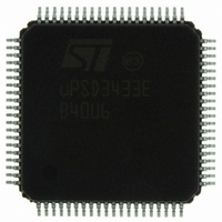
UPSD3433EB40U6 STMicroelectronics, UPSD3433EB40U6 Datasheet - Page 197

UPSD3433EB40U6
Manufacturer Part Number
UPSD3433EB40U6
Description
MCU 8BIT 8032 128KB FLASH 80TQFP
Manufacturer
STMicroelectronics
Series
µPSDr
Datasheet
1.UPSD3434EB40T6.pdf
(293 pages)
Specifications of UPSD3433EB40U6
Core Processor
8032
Core Size
8-Bit
Speed
40MHz
Connectivity
I²C, IrDA, SPI, UART/USART, USB
Peripherals
LVD, POR, PWM, WDT
Number Of I /o
46
Program Memory Size
160KB (160K x 8)
Program Memory Type
FLASH
Ram Size
8K x 8
Voltage - Supply (vcc/vdd)
3 V ~ 5.5 V
Data Converters
A/D 8x10b
Oscillator Type
Internal
Operating Temperature
-40°C ~ 85°C
Package / Case
80-TQFP, 80-VQFP
For Use With
497-5518 - EVAL BOARD RFID READER497-5046 - KIT TOOL FOR ST7/UPSD/STR7 MCU
Lead Free Status / RoHS Status
Lead free / RoHS Compliant
Eeprom Size
-
Other names
497-5660
Available stocks
Company
Part Number
Manufacturer
Quantity
Price
Company:
Part Number:
UPSD3433EB40U6
Manufacturer:
STMicroelectronics
Quantity:
10 000
- Current page: 197 of 293
- Download datasheet (5Mb)
uPSD34xx
28.2.7
Note:
Note:
1
2
The VM register
One of the csiop registers (the VM Register) controls whether or not the 8032 bus control
signals RD, WR, and PSEN are routed to the Main Flash memory, or the Secondary Flash
memory. Routing of these signals to these PSM Module memories determines if memories
reside in 8032 program address space, 8032 XDATA space, or both. The initial setting of the
VM Register is determined by a choice in PSDsoft Express and programmed into the
uPSD34xx in a non-volatile fashion using JTAG. This initial setting is loaded into the VM
Register upon power-up and also loaded upon any reset event. However, the 8032 may
override the initial VM Register setting at run-time by writing to the VM Register, which is
useful for IAP.
Table 104 on page 197
Bit 7, PIO_EN, is not related to the memory manipulation functions of Bits 1, 2, 3, and 4.
SRAM and csiop registers are always in XDATA space and cannot reside in program space.
Figure 70 on page 198
PSEN to the memories on the PSD Module. As an example, if we apply the value 0Ch to the
VM Register to implement the memory map example shown in
the routing of RD, WR, and PSEN would look like that shown in
In this example, the configuration is specified in PSDsoft Express and programmed into the
uPSD34xx using JTAG. Upon power-on or any reset condition, the non-volatile value 0Ch is
loaded into the VM Register. At runtime, the value 0Ch in the VM Register may be changed
(overridden) by the 8032 if desired to implement IAP or other functions.
Table 104. VM register (address = csiop + offset E2h)
Default value of Bits 1, 2, 3, and 4 is loaded from Non-Volatile setting as specified from
PSDsoft Express upon any reset or power-up condition. The default value of these bits can
be overridden by 8032 at run-time.
Default value of Bit 7 is zero upon any reset condition.
I/O Mode on
I/O Mode on
0 = disable
1 = enable
Peripheral
Peripheral
PIO_EN
Port A
Port A
Bit 7
Bit 6
used
used
not
not
illustrates how the VM Register affects the routing of RD, WR, and
defines bit functions within the VM Register.
Bit 5
used
used
not
not
Main Flash
WR cannot
Main Flash
Main Flash
0 = RD or
1 = RD or
WR can
XDATA
access
access
Space
Bit 4
Secondary
WR cannot
Secondary
Secondary
0 = RD or
1 = RD or
WR can
XDATA
access
access
Space
Flash
Flash
Flash
Bit 3
Main Flash
can access
Main Flash
Main Flash
0 = PSEN
1 = PSEN
Program
access
Space
cannot
Bit 2
Figure 64 on page
Figure 71 on page
Secondary
can access
Secondary
Secondary
0 = PSEN
1 = PSEN
Program
access
cannot
Space
Flash
Flash
Flash
Bit 1
PSD module
192, then
not used
not used
198.
Bit 0
197/293
Related parts for UPSD3433EB40U6
Image
Part Number
Description
Manufacturer
Datasheet
Request
R

Part Number:
Description:
MCU 8BIT 8032 128KB FLASH 80TQFP
Manufacturer:
STMicroelectronics
Datasheet:

Part Number:
Description:
MCU 8BIT 8032 128KB FLASH 52TQFP
Manufacturer:
STMicroelectronics
Datasheet:

Part Number:
Description:
STMicroelectronics [RIPPLE-CARRY BINARY COUNTER/DIVIDERS]
Manufacturer:
STMicroelectronics
Datasheet:

Part Number:
Description:
STMicroelectronics [LIQUID-CRYSTAL DISPLAY DRIVERS]
Manufacturer:
STMicroelectronics
Datasheet:

Part Number:
Description:
BOARD EVAL FOR MEMS SENSORS
Manufacturer:
STMicroelectronics
Datasheet:

Part Number:
Description:
NPN TRANSISTOR POWER MODULE
Manufacturer:
STMicroelectronics
Datasheet:

Part Number:
Description:
TURBOSWITCH ULTRA-FAST HIGH VOLTAGE DIODE
Manufacturer:
STMicroelectronics
Datasheet:

Part Number:
Description:
Manufacturer:
STMicroelectronics
Datasheet:

Part Number:
Description:
DIODE / SCR MODULE
Manufacturer:
STMicroelectronics
Datasheet:

Part Number:
Description:
DIODE / SCR MODULE
Manufacturer:
STMicroelectronics
Datasheet:

Part Number:
Description:
Search -----> STE16N100
Manufacturer:
STMicroelectronics
Datasheet:

Part Number:
Description:
Search ---> STE53NA50
Manufacturer:
STMicroelectronics
Datasheet:


