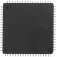
DF70845AD80FPV Renesas Electronics America, DF70845AD80FPV Datasheet - Page 42

DF70845AD80FPV
Manufacturer Part Number
DF70845AD80FPV
Description
IC SUPERH MCU FLASH 112LQFP
Manufacturer
Renesas Electronics America
Series
SuperH® SH7080r
Datasheet
1.DF70844AD80FPV.pdf
(1644 pages)
Specifications of DF70845AD80FPV
Core Size
32-Bit
Program Memory Size
512KB (512K x 8)
Core Processor
SH-2
Speed
80MHz
Connectivity
EBI/EMI, FIFO, I²C, SCI, SSU
Peripherals
DMA, POR, PWM, WDT
Number Of I /o
76
Program Memory Type
FLASH
Ram Size
32K x 8
Voltage - Supply (vcc/vdd)
3 V ~ 5.5 V
Data Converters
A/D 8x10b
Oscillator Type
Internal
Operating Temperature
-40°C ~ 85°C
Package / Case
112-LQFP
No. Of I/o's
76
Ram Memory Size
32KB
Cpu Speed
80MHz
Digital Ic Case Style
LQFP
Supply Voltage Range
3V To 3.6V, 4.5V To 5.5V
Embedded Interface Type
I2C, SCI
Rohs Compliant
Yes
Lead Free Status / RoHS Status
Lead free / RoHS Compliant
For Use With
R0K570865S001BE - KIT STARTER FOR SH7086R0K570865S000BE - KIT STARTER FOR SH7086HS0005KCU11H - EMULATOR E10A-USB H8S(X),SH2(A)
Eeprom Size
-
Lead Free Status / RoHS Status
Lead free / RoHS Compliant, Lead free / RoHS Compliant
Available stocks
Company
Part Number
Manufacturer
Quantity
Price
Company:
Part Number:
DF70845AD80FPV
Manufacturer:
TAIYO
Quantity:
40 000
Company:
Part Number:
DF70845AD80FPV
Manufacturer:
Renesas Electronics America
Quantity:
10 000
- Current page: 42 of 1644
- Download datasheet (10Mb)
Figure 23.11 Programming Procedure...................................................................................... 1258
Figure 23.12 Erasing Procedure ............................................................................................... 1263
Figure 23.13 Sample Procedure of Repeating RAM Emulation, Erasing, and Programming
Figure 23.14 Procedure for Programming User MAT in User Boot Mode .............................. 1267
Figure 23.15 Procedure for Erasing User MAT in User Boot Mode ........................................ 1269
Figure 23.16 Transitions to and from Error Protection State.................................................... 1273
Figure 23.17 Emulation of Flash Memory in RAM ................................................................. 1274
Figure 23.18 Example of Overlapped RAM Operation
Figure 23.19 Programming of Tuned Data (SH7083: 256-kbyte Flash Memory Version) ...... 1276
Figure 23.20 Switching between User MAT and User Boot MAT .......................................... 1278
Figure 23.21 Timing of Contention between SCO Download Request and Interrupt
Figure 23.22 Flow of Processing by the Boot Program............................................................ 1284
Figure 23.23 Sequence of Bit-Rate Matching........................................................................... 1285
Figure 23.24 Formats in the Communications Protocol ........................................................... 1286
Figure 23.25 Sequence of New Bit Rate Selection................................................................... 1298
Figure 23.26 Sequence of Programming .................................................................................. 1302
Figure 23.27 Sequence of Erasure ............................................................................................ 1306
Section 24 Mask ROM
Figure 24.1 Mask ROM Block Diagram .................................................................................. 1323
Section 25 RAM
Figure 25.1 On-chip RAM Addresses ...................................................................................... 1325
Section 28 Electrical Characteristics
Figure 28.1 EXTAL Clock Input Timing ................................................................................. 1412
Figure 28.2 CK Clock Output Timing ...................................................................................... 1413
Figure 28.3 Power-On Oscillation Settling Timing .................................................................. 1413
Figure 28.4 Oscillation Settling Timing on Return from Standby (Return by Reset)............... 1413
Figure 28.5 Oscillation Settling Timing on Return from Standby (Return by NMI or IRQ).... 1414
Figure 28.6 Reset Input Timing................................................................................................ 1416
Figure 28.7 Interrupt Signal Input Timing................................................................................ 1416
Figure 28.8 Interrupt Signal Output Timing ............................................................................. 1417
Figure 28.9 Bus Release Timing .............................................................................................. 1417
Figure 28.10 Pin Driving Timing in Standby Mode ................................................................. 1417
Figure 28.11 Basic Bus Timing for Normal Space (No Wait).................................................. 1421
Figure 28.12 Basic Bus Timing for Normal Space (One Software Wait Cycle) ...................... 1422
Figure 28.13 Basic Bus Timing for Normal Space (One External Wait Cycle) ....................... 1423
Rev. 3.00 May 17, 2007 Page xlii of Iviii
(Overview) .......................................................................................................... 1265
(SH7083: 256-kbyte Flash Memory Version) ..................................................... 1275
Request................................................................................................................ 1279
Related parts for DF70845AD80FPV
Image
Part Number
Description
Manufacturer
Datasheet
Request
R

Part Number:
Description:
KIT STARTER FOR M16C/29
Manufacturer:
Renesas Electronics America
Datasheet:

Part Number:
Description:
KIT STARTER FOR R8C/2D
Manufacturer:
Renesas Electronics America
Datasheet:

Part Number:
Description:
R0K33062P STARTER KIT
Manufacturer:
Renesas Electronics America
Datasheet:

Part Number:
Description:
KIT STARTER FOR R8C/23 E8A
Manufacturer:
Renesas Electronics America
Datasheet:

Part Number:
Description:
KIT STARTER FOR R8C/25
Manufacturer:
Renesas Electronics America
Datasheet:

Part Number:
Description:
KIT STARTER H8S2456 SHARPE DSPLY
Manufacturer:
Renesas Electronics America
Datasheet:

Part Number:
Description:
KIT STARTER FOR R8C38C
Manufacturer:
Renesas Electronics America
Datasheet:

Part Number:
Description:
KIT STARTER FOR R8C35C
Manufacturer:
Renesas Electronics America
Datasheet:

Part Number:
Description:
KIT STARTER FOR R8CL3AC+LCD APPS
Manufacturer:
Renesas Electronics America
Datasheet:

Part Number:
Description:
KIT STARTER FOR RX610
Manufacturer:
Renesas Electronics America
Datasheet:

Part Number:
Description:
KIT STARTER FOR R32C/118
Manufacturer:
Renesas Electronics America
Datasheet:

Part Number:
Description:
KIT DEV RSK-R8C/26-29
Manufacturer:
Renesas Electronics America
Datasheet:

Part Number:
Description:
KIT STARTER FOR SH7124
Manufacturer:
Renesas Electronics America
Datasheet:

Part Number:
Description:
KIT STARTER FOR H8SX/1622
Manufacturer:
Renesas Electronics America
Datasheet:

Part Number:
Description:
KIT DEV FOR SH7203
Manufacturer:
Renesas Electronics America
Datasheet:


