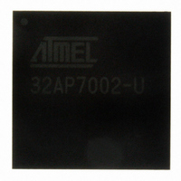
AT32AP7002-CTUT Atmel, AT32AP7002-CTUT Datasheet - Page 749

AT32AP7002-CTUT
Manufacturer Part Number
AT32AP7002-CTUT
Description
IC MCU 32BIT AVR32 196-CBGA
Manufacturer
Atmel
Series
AVR®32 AP7r
Specifications of AT32AP7002-CTUT
Core Processor
AVR
Core Size
32-Bit
Speed
150MHz
Connectivity
EBI/EMI, I²C, MMC, PS2, SPI, SSC, UART/USART, USB
Peripherals
AC'97, DMA, I²C, LCD, POR, PWM, WDT
Number Of I /o
85
Program Memory Type
ROMless
Ram Size
32K x 8
Voltage - Supply (vcc/vdd)
1.65 V ~ 1.95 V
Data Converters
D/A 2x16b
Oscillator Type
Internal
Operating Temperature
-40°C ~ 85°C
Package / Case
196-CBGA
Data Bus Width
32 bit
Data Ram Size
32 KB
Interface Type
I2C, JTAG, PS2, SPI, SSC, UART, USART, USB
Maximum Clock Frequency
150 MHz
Number Of Timers
3
Maximum Operating Temperature
+ 85 C
Mounting Style
SMD/SMT
Minimum Operating Temperature
- 40 C
On-chip Dac
16 bit, 2 Channel
Package
196CTBGA
Device Core
AVR32
Family Name
AT32
Maximum Speed
150 MHz
Operating Supply Voltage
1.8|3.3 V
For Use With
ATAVRONEKIT - KIT AVR/AVR32 DEBUGGER/PROGRMMRATNGW100 - KIT AVR32 NETWORK GATEWAYATSTK1000 - KIT STARTER FOR AVR32AP7000
Lead Free Status / RoHS Status
Lead free / RoHS Compliant
Eeprom Size
-
Program Memory Size
-
Lead Free Status / Rohs Status
Details
Available stocks
Company
Part Number
Manufacturer
Quantity
Price
- Current page: 749 of 896
- Download datasheet (13Mb)
34.6.2.9
32054F–AVR32–09/09
Equation 1
Table 34-11. Minimum PCLK Period in LCDC Core Clock Cycles
The DVAL signal indicates valid data in the LCD Interface.
After each horizontal line of data has been shifted into the LCD, the HSYNC is asserted to cause
the line to be displayed on the panel.
The following timing parameters can be configured:
There is a limitation in the minimum values of VHDLY, HPW and HBP parameters imposed by
the initial latency of the datapath. The total delay in LCDC Core Clock cycles must be higher
than or equal to the latency column in
lowing formula:
where:
The VSYNC is asserted once per frame. This signal is asserted to cause the LCD's line pointer
to start over at the top of the display. The timing of this signal depends on the type of LCD: STN
or TFT LCD.
In STN mode, the high phase corresponds to the complete first line of the frame. In STN mode,
this signal is synchronized with the first active PCLK rising edge in a line.
In TFT mode, the high phase of this signal starts at the beginning of the first line. The following
timing parameters can be selected:
DISTYPE
STN Color
STN Color
STN Color
•Vertical to Horizontal Delay (VHDLY): The delay between begin_of_line and the generation of
•Horizontal Pulse Width (HPW): The HSYNC pulse width is configurable in HPW field of
•Horizontal Back Porch (HBP): The delay between the HSYNC falling edge and the first PCLK
•Horizontal Front Porch (HFP): The delay between end of valid data and the end of the line is
•VHDLY, HPW, HBP are the value of the fields of LCDTIM1 and LCDTIM2 registers
•PCLK_PERIOD is the period of PCLK signal measured in LCDC Core Clock cycles
•DPATH_LATENCY is the datapath latency of the configuration, given in
•Vertical Pulse Width (VPW): VSYNC pulse width is configurable in VPW field of the LCDTIM1
HSYNC is configurable in the VHDLY field of the LCDTIM1 register. The delay is equal to
(VHDLY+1) PCLK cycles.
LCDTIM2 register. The width is equal to (HPW + 1) PCLK cycles.
rising edge with valid data at the LCD Interface is configurable in the HBP field of the
LCDTIM2 register. The delay is equal to (HBP+1) PCLK cycles.
configurable in the HFP field of the LCDTIM2 register. The delay is equal to (HFP+1) PCLK
cycles.
741
register. The pulse width is equal to (VPW+1) lines.
(
VHDLY
+
SCAN
Single
Dual
Dual
HPW
Configuration
+
HBP
Table 34-2 on page
+
3
)
×
PCLK_PERIOD
IFWIDTH
8
8
16
741. This limitation is given by the fol-
≥
DPATH_LATENCY
AT32AP7002
PCLK Period
2
4
6
Table 34-2 on page
749
Related parts for AT32AP7002-CTUT
Image
Part Number
Description
Manufacturer
Datasheet
Request
R

Part Number:
Description:
DEV KIT FOR AVR/AVR32
Manufacturer:
Atmel
Datasheet:

Part Number:
Description:
INTERVAL AND WIPE/WASH WIPER CONTROL IC WITH DELAY
Manufacturer:
ATMEL Corporation
Datasheet:

Part Number:
Description:
Low-Voltage Voice-Switched IC for Hands-Free Operation
Manufacturer:
ATMEL Corporation
Datasheet:

Part Number:
Description:
MONOLITHIC INTEGRATED FEATUREPHONE CIRCUIT
Manufacturer:
ATMEL Corporation
Datasheet:

Part Number:
Description:
AM-FM Receiver IC U4255BM-M
Manufacturer:
ATMEL Corporation
Datasheet:

Part Number:
Description:
Monolithic Integrated Feature Phone Circuit
Manufacturer:
ATMEL Corporation
Datasheet:

Part Number:
Description:
Multistandard Video-IF and Quasi Parallel Sound Processing
Manufacturer:
ATMEL Corporation
Datasheet:

Part Number:
Description:
High-performance EE PLD
Manufacturer:
ATMEL Corporation
Datasheet:

Part Number:
Description:
8-bit Flash Microcontroller
Manufacturer:
ATMEL Corporation
Datasheet:

Part Number:
Description:
2-Wire Serial EEPROM
Manufacturer:
ATMEL Corporation
Datasheet:


