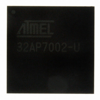
AT32AP7002-CTUT Atmel, AT32AP7002-CTUT Datasheet - Page 20

AT32AP7002-CTUT
Manufacturer Part Number
AT32AP7002-CTUT
Description
IC MCU 32BIT AVR32 196-CBGA
Manufacturer
Atmel
Series
AVR®32 AP7r
Specifications of AT32AP7002-CTUT
Core Processor
AVR
Core Size
32-Bit
Speed
150MHz
Connectivity
EBI/EMI, I²C, MMC, PS2, SPI, SSC, UART/USART, USB
Peripherals
AC'97, DMA, I²C, LCD, POR, PWM, WDT
Number Of I /o
85
Program Memory Type
ROMless
Ram Size
32K x 8
Voltage - Supply (vcc/vdd)
1.65 V ~ 1.95 V
Data Converters
D/A 2x16b
Oscillator Type
Internal
Operating Temperature
-40°C ~ 85°C
Package / Case
196-CBGA
Data Bus Width
32 bit
Data Ram Size
32 KB
Interface Type
I2C, JTAG, PS2, SPI, SSC, UART, USART, USB
Maximum Clock Frequency
150 MHz
Number Of Timers
3
Maximum Operating Temperature
+ 85 C
Mounting Style
SMD/SMT
Minimum Operating Temperature
- 40 C
On-chip Dac
16 bit, 2 Channel
Package
196CTBGA
Device Core
AVR32
Family Name
AT32
Maximum Speed
150 MHz
Operating Supply Voltage
1.8|3.3 V
For Use With
ATAVRONEKIT - KIT AVR/AVR32 DEBUGGER/PROGRMMRATNGW100 - KIT AVR32 NETWORK GATEWAYATSTK1000 - KIT STARTER FOR AVR32AP7000
Lead Free Status / RoHS Status
Lead free / RoHS Compliant
Eeprom Size
-
Program Memory Size
-
Lead Free Status / Rohs Status
Details
Available stocks
Company
Part Number
Manufacturer
Quantity
Price
- Current page: 20 of 896
- Download datasheet (13Mb)
6.2.5
6.2.6
32054F–AVR32–09/09
Caches and write buffer
Unaligned reference handling
AVR32 AP implements 16K data and 16K instruction caches. The caches are 4-way set asso-
ciative. Each cache has a 32-bit System Bus master interface connecting it to the bus. The
instruction cache has a 32-bit interface to the fetch pipeline stage, and the data cache has a 64-
bit interface to the load-store pipeline. The caches use a least recently used allocate-on-read-
miss replacement policy. The caches are virtually tagged, physically indexed, avoiding the need
to flush them on task switch.
The caches provide locking on a per-line basis, allowing code and data to be permanently
locked in the caches for timing-critical code. The data cache also allows prefetching of data
using the pref instruction.
Accesses to the instruction and data caches are tagged as cacheable or uncacheable on a per-
page basis by the MMU. Data cache writes are tagged as write-through or writeback on a per-
page basis by the MMU.
The data cache has a 32-byte combining write buffer, to avoid stalling the CPU when writing to
external memory. Writes are tagged as bufferable or unbufferable on a per-page basis by the
MMU. Bufferable writes to sequential addresses are placed in the buffer, allowing for example a
sequence of byte writes from the CPU to be combined into word transfers on the bus. A sync
instruction is provided to explicitly flush the write buffer.
AVR32 AP has hardware support for performing unaligned memory accesses. This will reduce
the memory footprint needed by some applications, as well as speed up other applications oper-
ating on unaligned data.
AVR32 AP is able to perform certain word-sized load and store instructions of any alignment,
and word-aligned st.d and ld.d. Any other unaligned memory access will cause an MMU address
exception. All coprocessor memory access instructions require word-aligned pointers. Double-
word-sized accesses with word-aligned pointers will automatically be performed as two word-
sized accesses.
The following table shows the instructions with support for unaligned addresses. All other
instructions require aligned addresses. Accessing an unaligned address may require several
clock cycles, refer to the AVR32 AP Technical Reference Manual for details.
Table 6-1.
Instruction
ld.w
st.w
lddsp
lddpc
stdsp
ld.d
st.d
All coprocessor memory access instruction
Instructions with unaligned reference support
Supported alignment
Any
Any
Any
Any
Any
Word
Word
Word
AT32AP7002
20
Related parts for AT32AP7002-CTUT
Image
Part Number
Description
Manufacturer
Datasheet
Request
R

Part Number:
Description:
DEV KIT FOR AVR/AVR32
Manufacturer:
Atmel
Datasheet:

Part Number:
Description:
INTERVAL AND WIPE/WASH WIPER CONTROL IC WITH DELAY
Manufacturer:
ATMEL Corporation
Datasheet:

Part Number:
Description:
Low-Voltage Voice-Switched IC for Hands-Free Operation
Manufacturer:
ATMEL Corporation
Datasheet:

Part Number:
Description:
MONOLITHIC INTEGRATED FEATUREPHONE CIRCUIT
Manufacturer:
ATMEL Corporation
Datasheet:

Part Number:
Description:
AM-FM Receiver IC U4255BM-M
Manufacturer:
ATMEL Corporation
Datasheet:

Part Number:
Description:
Monolithic Integrated Feature Phone Circuit
Manufacturer:
ATMEL Corporation
Datasheet:

Part Number:
Description:
Multistandard Video-IF and Quasi Parallel Sound Processing
Manufacturer:
ATMEL Corporation
Datasheet:

Part Number:
Description:
High-performance EE PLD
Manufacturer:
ATMEL Corporation
Datasheet:

Part Number:
Description:
8-bit Flash Microcontroller
Manufacturer:
ATMEL Corporation
Datasheet:

Part Number:
Description:
2-Wire Serial EEPROM
Manufacturer:
ATMEL Corporation
Datasheet:


