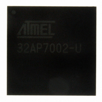
AT32AP7002-CTUT Atmel, AT32AP7002-CTUT Datasheet - Page 174

AT32AP7002-CTUT
Manufacturer Part Number
AT32AP7002-CTUT
Description
IC MCU 32BIT AVR32 196-CBGA
Manufacturer
Atmel
Series
AVR®32 AP7r
Specifications of AT32AP7002-CTUT
Core Processor
AVR
Core Size
32-Bit
Speed
150MHz
Connectivity
EBI/EMI, I²C, MMC, PS2, SPI, SSC, UART/USART, USB
Peripherals
AC'97, DMA, I²C, LCD, POR, PWM, WDT
Number Of I /o
85
Program Memory Type
ROMless
Ram Size
32K x 8
Voltage - Supply (vcc/vdd)
1.65 V ~ 1.95 V
Data Converters
D/A 2x16b
Oscillator Type
Internal
Operating Temperature
-40°C ~ 85°C
Package / Case
196-CBGA
Data Bus Width
32 bit
Data Ram Size
32 KB
Interface Type
I2C, JTAG, PS2, SPI, SSC, UART, USART, USB
Maximum Clock Frequency
150 MHz
Number Of Timers
3
Maximum Operating Temperature
+ 85 C
Mounting Style
SMD/SMT
Minimum Operating Temperature
- 40 C
On-chip Dac
16 bit, 2 Channel
Package
196CTBGA
Device Core
AVR32
Family Name
AT32
Maximum Speed
150 MHz
Operating Supply Voltage
1.8|3.3 V
For Use With
ATAVRONEKIT - KIT AVR/AVR32 DEBUGGER/PROGRMMRATNGW100 - KIT AVR32 NETWORK GATEWAYATSTK1000 - KIT STARTER FOR AVR32AP7000
Lead Free Status / RoHS Status
Lead free / RoHS Compliant
Eeprom Size
-
Program Memory Size
-
Lead Free Status / Rohs Status
Details
Available stocks
Company
Part Number
Manufacturer
Quantity
Price
- Current page: 174 of 896
- Download datasheet (13Mb)
17.8.2.1
Figure 17-6. External DMA Request Timing
17.9
32054F–AVR32–09/09
nDMAREQx
DMACA Transfer Types
dma_ack
dma_req
Hclk
External DMA Request Definition
When an external slave peripheral requires the DMACA to perform DMA transactions, it commu-
nicates its request by asserting the external nDMAREQx signal. This signal is resynchronized to
ensure a proper functionality (see
The external nDMAREQx signal should be asserted when the source threshold level is reached.
After resynchronization, the rising edge of dma_req starts the transfer.
The external nDMAREQx signal must be de-asserted after the last transfer and re-asserted
again before a new transaction starts.
For a source FIFO, an active edge should be triggered on nDMAREQx when the source FIFO
exceeds a watermark level. For a destination FIFO, an active edge should be triggered on
nDMAREQx when the destination FIFO drops below the watermark level.
The source transaction length, CTLx.SRC_MSIZE, and destination transaction length,
CTLx.DEST_MSIZE, must be set according to watermark levels on the source/destination
peripherals.
A DMA transfer may consist of single or multi-block transfers. On successive blocks of a multi-
block transfer, the SARx/DARx register in the DMACA is reprogrammed using either of the fol-
lowing methods:
• Block chaining using linked lists
• Auto-reloading
• Contiguous address between blocks
On successive blocks of a multi-block transfer, the CTLx register in the DMACA is re-pro-
grammed using either of the following methods:
• Block chaining using linked lists
• Auto-reloading
When block chaining, using linked lists is the multi-block method of choice, and on successive
blocks, the LLPx register in the DMACA is re-programmed using the following method:
• Block chaining using linked lists
DMA Transfers
DMA Transaction
DMA Transfers
”External DMA Request Timing” on page
DMA Transfers
AT32AP7002
174).
174
Related parts for AT32AP7002-CTUT
Image
Part Number
Description
Manufacturer
Datasheet
Request
R

Part Number:
Description:
DEV KIT FOR AVR/AVR32
Manufacturer:
Atmel
Datasheet:

Part Number:
Description:
INTERVAL AND WIPE/WASH WIPER CONTROL IC WITH DELAY
Manufacturer:
ATMEL Corporation
Datasheet:

Part Number:
Description:
Low-Voltage Voice-Switched IC for Hands-Free Operation
Manufacturer:
ATMEL Corporation
Datasheet:

Part Number:
Description:
MONOLITHIC INTEGRATED FEATUREPHONE CIRCUIT
Manufacturer:
ATMEL Corporation
Datasheet:

Part Number:
Description:
AM-FM Receiver IC U4255BM-M
Manufacturer:
ATMEL Corporation
Datasheet:

Part Number:
Description:
Monolithic Integrated Feature Phone Circuit
Manufacturer:
ATMEL Corporation
Datasheet:

Part Number:
Description:
Multistandard Video-IF and Quasi Parallel Sound Processing
Manufacturer:
ATMEL Corporation
Datasheet:

Part Number:
Description:
High-performance EE PLD
Manufacturer:
ATMEL Corporation
Datasheet:

Part Number:
Description:
8-bit Flash Microcontroller
Manufacturer:
ATMEL Corporation
Datasheet:

Part Number:
Description:
2-Wire Serial EEPROM
Manufacturer:
ATMEL Corporation
Datasheet:


