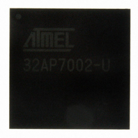
AT32AP7002-CTUT Atmel, AT32AP7002-CTUT Datasheet - Page 177

AT32AP7002-CTUT
Manufacturer Part Number
AT32AP7002-CTUT
Description
IC MCU 32BIT AVR32 196-CBGA
Manufacturer
Atmel
Series
AVR®32 AP7r
Specifications of AT32AP7002-CTUT
Core Processor
AVR
Core Size
32-Bit
Speed
150MHz
Connectivity
EBI/EMI, I²C, MMC, PS2, SPI, SSC, UART/USART, USB
Peripherals
AC'97, DMA, I²C, LCD, POR, PWM, WDT
Number Of I /o
85
Program Memory Type
ROMless
Ram Size
32K x 8
Voltage - Supply (vcc/vdd)
1.65 V ~ 1.95 V
Data Converters
D/A 2x16b
Oscillator Type
Internal
Operating Temperature
-40°C ~ 85°C
Package / Case
196-CBGA
Data Bus Width
32 bit
Data Ram Size
32 KB
Interface Type
I2C, JTAG, PS2, SPI, SSC, UART, USART, USB
Maximum Clock Frequency
150 MHz
Number Of Timers
3
Maximum Operating Temperature
+ 85 C
Mounting Style
SMD/SMT
Minimum Operating Temperature
- 40 C
On-chip Dac
16 bit, 2 Channel
Package
196CTBGA
Device Core
AVR32
Family Name
AT32
Maximum Speed
150 MHz
Operating Supply Voltage
1.8|3.3 V
For Use With
ATAVRONEKIT - KIT AVR/AVR32 DEBUGGER/PROGRMMRATNGW100 - KIT AVR32 NETWORK GATEWAYATSTK1000 - KIT STARTER FOR AVR32AP7000
Lead Free Status / RoHS Status
Lead free / RoHS Compliant
Eeprom Size
-
Program Memory Size
-
Lead Free Status / Rohs Status
Details
Available stocks
Company
Part Number
Manufacturer
Quantity
Price
- Current page: 177 of 896
- Download datasheet (13Mb)
17.9.1.4
17.9.2
32054F–AVR32–09/09
Ending Multi-block Transfers
Suspension of Transfers Between Blocks
blocks is a function of CTLx.LLP_S_EN, CFGx.RELOAD_SR, CTLx.LLP_D_EN, and
CFGx.RELOAD_DS registers (see
Note:
At the end of every block transfer, an end of block interrupt is asserted if:
• interrupts are enabled, CTLx.INT_EN = 1
• the channel block interrupt is unmasked, MaskBlock[n] = 0, where n is the channel number.
Note:
For rows 6, 8, and 10 of
transfers. For example, at the end of block N, the DMACA automatically proceeds to block N + 1.
For rows 2, 3, 4, 7, and 9 of
block transfers), the DMA transfer automatically stalls after the end of block. Interrupt is asserted
if the end of block interrupt is enabled and unmasked.
The DMACA does not proceed to the next block transfer until a write to the block interrupt clear
register, ClearBlock[n], is performed by software. This clears the channel block complete
interrupt.
For rows 2, 3, 4, 7, and 9 of
block transfers), the DMA transfer does not stall if either:
• interrupts are disabled, CTLx.INT_EN = 0, or
• the channel block interrupt is masked, MaskBlock[n] = 1, where n is the channel number.
Channel suspension between blocks is used to ensure that the end of block ISR (interrupt ser-
vice routine) of the next-to-last block is serviced before the start of the final block commences.
This ensures that the ISR has cleared the CFGx.RELOAD_SR and/or CFGx.RELOAD_DS bits
b efo re co mp let ion of t he fina l blo ck. Th e r elo ad bit s CFGx .REL OAD _SR a nd /o r
CFGx.RELOAD_DS should be cleared in the ‘end of block ISR’ for the next-to-last block
transfer.
All multi-block transfers must end as shown in either Row 1 or Row 5 of
At the end of every block transfer, the DMACA samples the row number, and if the DMACA is in
Row 1 or Row 5 state, then the previous block transferred was the last block and the DMA trans-
fer is terminated.
Note:
For rows 2,3 and 4 of
C F G x . R E L O A D _ D S i s s e t ) , m u l t i - b l o c k D M A t r a n s f e r s c o n t i n u e u n t i l b o t h t h e
CFGx.RELOAD_SR and CFGx.RELOAD_DS registers are cleared by software. They should be
Both SARx and DARx updates cannot be selected to be contiguous. If this functionality is
required, the size of the Block Transfer (CTLx.BLOCK_TS) must be increased. If this is at the max-
imum value, use Row 10 of
block descriptor to be equal to the end SARx address of the previous block. Similarly, setup the
LLI.DARx address of the block descriptor to be equal to the end DARx address of the previous
block.
The block complete interrupt is generated at the completion of the block transfer to the destination.
Row 1 and Row 5 are used for single block transfers or terminating multiblock transfers. Ending in
Row 5 state enables status fetch for the last block. Ending in Row 1 state disables status fetch for
the last block.
Table 17-1 on page
Table 17-1 on page
Table 17-1 on page 176
Table 17-1 on page 176
Table 17-1 on page 176
Figure 17-1 on page
176, the DMA transfer does not stall between block
176, (LLPx = 0 and CFGx.RELOAD_SR and/or
(SARx and/or DARx auto-reloaded between
(SARx and/or DARx auto-reloaded between
166).
and setup the LLI.SARx address of the
AT32AP7002
Table 17-1 on page
176.
177
Related parts for AT32AP7002-CTUT
Image
Part Number
Description
Manufacturer
Datasheet
Request
R

Part Number:
Description:
DEV KIT FOR AVR/AVR32
Manufacturer:
Atmel
Datasheet:

Part Number:
Description:
INTERVAL AND WIPE/WASH WIPER CONTROL IC WITH DELAY
Manufacturer:
ATMEL Corporation
Datasheet:

Part Number:
Description:
Low-Voltage Voice-Switched IC for Hands-Free Operation
Manufacturer:
ATMEL Corporation
Datasheet:

Part Number:
Description:
MONOLITHIC INTEGRATED FEATUREPHONE CIRCUIT
Manufacturer:
ATMEL Corporation
Datasheet:

Part Number:
Description:
AM-FM Receiver IC U4255BM-M
Manufacturer:
ATMEL Corporation
Datasheet:

Part Number:
Description:
Monolithic Integrated Feature Phone Circuit
Manufacturer:
ATMEL Corporation
Datasheet:

Part Number:
Description:
Multistandard Video-IF and Quasi Parallel Sound Processing
Manufacturer:
ATMEL Corporation
Datasheet:

Part Number:
Description:
High-performance EE PLD
Manufacturer:
ATMEL Corporation
Datasheet:

Part Number:
Description:
8-bit Flash Microcontroller
Manufacturer:
ATMEL Corporation
Datasheet:

Part Number:
Description:
2-Wire Serial EEPROM
Manufacturer:
ATMEL Corporation
Datasheet:


