AT91SAM9G45-EKES Atmel, AT91SAM9G45-EKES Datasheet - Page 938
AT91SAM9G45-EKES
Manufacturer Part Number
AT91SAM9G45-EKES
Description
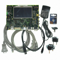
KIT EVAL FOR AT91SAM9G45
Manufacturer
Atmel
Series
AT91SAM Smart ARMr
Type
MCUr
Datasheets
1.AT91SAM9G45-EKES.pdf
(56 pages)
2.AT91SAM9G45-EKES.pdf
(1218 pages)
3.AT91SAM9G45-EKES.pdf
(66 pages)
Specifications of AT91SAM9G45-EKES
Contents
Board
Processor To Be Evaluated
SAM9G45
Data Bus Width
32 bit
Interface Type
I2C, SPI, UART
Maximum Operating Temperature
+ 50 C
Minimum Operating Temperature
- 10 C
Operating Supply Voltage
1.8 V to 3.3 V
For Use With/related Products
AT91SAM9G45
Lead Free Status / RoHS Status
Lead free / RoHS Compliant
Other names
Q4626953


40.5.5
40.6
40.6.1
40.6.2
40.6.3
938
Analog-to-digital Converter Functional Description
AT91SAM9G45
Conversion Performances
ADC Resolution
ADC Clock
Sleep Mode
For performance and electrical characteristics of the TSADCC, see the section “Electrical Char-
acteristics” of the full datasheet.
The TSADCC embeds a Successive Approximation Register (SAR) Analog-to-Digital Converter
(ADC). The ADC supports 8-bit or 10-bit resolutions.
The conversion is performed on a full range between 0V and the reference voltage pin TSAD-
VREF. Analog inputs between these voltages convert to values based on a linear conversion.
The ADC supports 8-bit or 10-bit resolutions. The 8-bit selection is performed by setting the bit
LOWRES in the TSADCC Mode Register. See
page
By default, after a reset, the resolution is the highest and the DATA field in the
nel Data Register x (x = 0..7)”
By setting the bit LOWRES, the ADC switches in the lowest resolution and the conversion
results can be read in the eight lowest significant bits of the data registers. The two highest bits
of the DATA field in the corresponding TSADCC_CDR register and of the LDATA field in the
TSADCC_LCDR register read 0.
Moreover, when a PDC channel is connected to the TSADCC, 10-bit resolution sets the transfer
request sizes to 16-bit. Setting the bit LOWRES automatically switches to 8-bit data transfers. In
this case, the destination buffers are optimized.
All the conversions for the Touch Screen forces the ADC in 10-bit resolution, regardless of the
LOWRES setting. Further details are given in the section
The TSADCC uses the ADC Clock to perform conversions. Converting a single analog value to
a 10-bit digital data requires Sample and Hold Clock cycles as defined in the field SHTIM of the
“TSADCC Mode Register”
the PRESCAL field of the
The ADC clock range is between MCK/2, if PRESCAL is 0, and MCK/128, if PRESCAL is set to
63 (0x3F). PRESCAL must be programmed in order to provide an ADC clock frequency accord-
ing to the maximum sampling rate parameter given in the Electrical Characteristics section.
The TSADCC Sleep Mode maximizes power saving by automatically deactivating the Analog-to-
Digital Converter cell when it is not being used for conversions. Sleep Mode is enabled by set-
ting the bit SLEEP in
The SLEEP of the ADC is automatically managed by the conversion sequencer, which can auto-
matically process the conversions of all channels at lowest power consumption.
When a trigger occurs, the Analog-to-Digital Converter cell is automatically activated. As the
analog cell requires a start-up time, the logic waits during this time and then starts the conver-
sion on the enabled channels. When all conversions are complete, the ADC is deactivated until
the next trigger.
956.
“TSADCC Mode
“TSADCC Mode
and 10 ADC Clock cycles. The ADC Clock frequency is selected in
are fully used.
Register”.
Register”.
Section 40.11.2 “TSADCC Mode Register” on
“Operating Modes” on page
6438F–ATARM–21-Jun-10
“TSADCC Chan-
946.
Related parts for AT91SAM9G45-EKES
Image
Part Number
Description
Manufacturer
Datasheet
Request
R

Part Number:
Description:
MCU ARM9 64K SRAM 144-LFBGA
Manufacturer:
Atmel
Datasheet:

Part Number:
Description:
IC ARM7 MCU FLASH 256K 100LQFP
Manufacturer:
Atmel
Datasheet:

Part Number:
Description:
IC ARM9 MPU 217-LFBGA
Manufacturer:
Atmel
Datasheet:
Part Number:
Description:
MCU ARM9 ULTRA LOW PWR 217-LFBGA
Manufacturer:
Atmel
Datasheet:

Part Number:
Description:
MCU ARM9 324-TFBGA
Manufacturer:
Atmel
Datasheet:
Part Number:
Description:
IC MCU ARM9 SAMPLING 217CBGA
Manufacturer:
Atmel
Datasheet:
Part Number:
Description:
IC ARM9 MCU 217-LFBGA
Manufacturer:
Atmel
Datasheet:

Part Number:
Description:
IC ARM9 MCU 208-PQFP
Manufacturer:
Atmel
Datasheet:
Part Number:
Description:
MCU ARM 512K HS FLASH 100-LQFP
Manufacturer:
Atmel
Datasheet:

Part Number:
Description:
MCU ARM 512K HS FLASH 100-TFBGA
Manufacturer:
Atmel
Datasheet:
Part Number:
Description:
IC ARM9 MCU 200 MHZ 324-TFBGA
Manufacturer:
Atmel
Datasheet:

Part Number:
Description:
IC ARM MCU 16BIT 128K 256BGA
Manufacturer:
Atmel
Datasheet:

Part Number:
Description:
IC ARM7 MCU 32BIT 128K 64LQFP
Manufacturer:
Atmel
Datasheet:

Part Number:
Description:
IC ARM7 MCU FLASH 256K 128-LQFP
Manufacturer:
Atmel
Datasheet:
Part Number:
Description:
IC ARM7 MCU FLASH 512K 128-LQFP
Manufacturer:
Atmel
Datasheet: