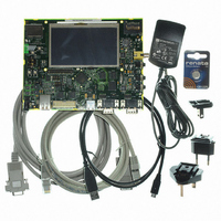
AT91SAM9G45-EKES Atmel, AT91SAM9G45-EKES Datasheet - Page 1122

AT91SAM9G45-EKES
Manufacturer Part Number
AT91SAM9G45-EKES
Description
KIT EVAL FOR AT91SAM9G45
Manufacturer
Atmel
Series
AT91SAM Smart ARMr
Type
MCUr
Datasheets
1.AT91SAM9G45-EKES.pdf
(56 pages)
2.AT91SAM9G45-EKES.pdf
(1218 pages)
3.AT91SAM9G45-EKES.pdf
(66 pages)
Specifications of AT91SAM9G45-EKES
Contents
Board
Processor To Be Evaluated
SAM9G45
Data Bus Width
32 bit
Interface Type
I2C, SPI, UART
Maximum Operating Temperature
+ 50 C
Minimum Operating Temperature
- 10 C
Operating Supply Voltage
1.8 V to 3.3 V
For Use With/related Products
AT91SAM9G45
Lead Free Status / RoHS Status
Lead free / RoHS Compliant
Other names
Q4626953
- Current page: 1122 of 1218
- Download datasheet (19Mb)
45.9
45.10 2D Memory Addressing
Figure 45-13. Frame Buffer Addressing
1122
Double-buffer Technique
AT91SAM9G45
The double-buffer technique is used to avoid flickering while the frame being displayed is
updated. Instead of using a single buffer, there are two different buffers, the backbuffer (back-
ground buffer) and the primary buffer (the buffer being displayed).
The host updates the backbuffer while the LCD Controller is displaying the primary buffer. When
the backbuffer has been updated the host updates the DMA Base Address registers.
When using a Dual Panel LCD Module, both base address pointers should be updated in the
same frame. There are two possibilities:
Once the host has updated the Frame Base Address Registers and the next DMA end of frame
IRQ arrives, the backbuffer and the primary buffer are swapped and the host can work with the
new backbuffer.
When using a dual-panel LCD module, both base address pointers should be updated in the
same frame. In order to achieve this, the DMAUPDT bit in DMACON register must be used to
validate the new base address.
The LCDC can be configured to work on a frame buffer larger than the actual screen size. By
changing the values in a few registers, it is easy to move the displayed area along the frame buf-
fer width and height.
In order to locate the displayed window within a larger frame buffer, the software must:
• Check the DMAFRMPTx register to ensure that there is enough time to update the DMA
• Update the Frame Base Address Registers when the End Of Frame IRQ is generated.
• Program the DMABADDR1 (DMABADDR2) register(s) to make them point to the word
• Program the PIXELOFF field of DMA2DCFG register to specify the offset of this first pixel
Base Address registers before the end of frame.
containing the first pixel of the area of interest.
within the 32-bit memory word that contains it.
Base word address &
pixel offset
Line-to-line
address increment
Frame Buffer
Displayed Image
6438F–ATARM–21-Jun-10
Related parts for AT91SAM9G45-EKES
Image
Part Number
Description
Manufacturer
Datasheet
Request
R

Part Number:
Description:
MCU ARM9 64K SRAM 144-LFBGA
Manufacturer:
Atmel
Datasheet:

Part Number:
Description:
IC ARM7 MCU FLASH 256K 100LQFP
Manufacturer:
Atmel
Datasheet:

Part Number:
Description:
IC ARM9 MPU 217-LFBGA
Manufacturer:
Atmel
Datasheet:

Part Number:
Description:
MCU ARM9 ULTRA LOW PWR 217-LFBGA
Manufacturer:
Atmel
Datasheet:

Part Number:
Description:
MCU ARM9 324-TFBGA
Manufacturer:
Atmel
Datasheet:

Part Number:
Description:
IC MCU ARM9 SAMPLING 217CBGA
Manufacturer:
Atmel
Datasheet:

Part Number:
Description:
IC ARM9 MCU 217-LFBGA
Manufacturer:
Atmel
Datasheet:

Part Number:
Description:
IC ARM9 MCU 208-PQFP
Manufacturer:
Atmel
Datasheet:

Part Number:
Description:
MCU ARM 512K HS FLASH 100-LQFP
Manufacturer:
Atmel
Datasheet:

Part Number:
Description:
MCU ARM 512K HS FLASH 100-TFBGA
Manufacturer:
Atmel
Datasheet:

Part Number:
Description:
IC ARM9 MCU 200 MHZ 324-TFBGA
Manufacturer:
Atmel
Datasheet:

Part Number:
Description:
IC ARM MCU 16BIT 128K 256BGA
Manufacturer:
Atmel
Datasheet:

Part Number:
Description:
IC ARM7 MCU 32BIT 128K 64LQFP
Manufacturer:
Atmel
Datasheet:

Part Number:
Description:
IC ARM7 MCU FLASH 256K 128-LQFP
Manufacturer:
Atmel
Datasheet:

Part Number:
Description:
IC ARM7 MCU FLASH 512K 128-LQFP
Manufacturer:
Atmel
Datasheet:


