AT91SAM9G45-EKES Atmel, AT91SAM9G45-EKES Datasheet - Page 192
AT91SAM9G45-EKES
Manufacturer Part Number
AT91SAM9G45-EKES
Description
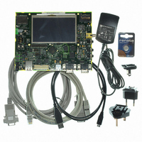
KIT EVAL FOR AT91SAM9G45
Manufacturer
Atmel
Series
AT91SAM Smart ARMr
Type
MCUr
Datasheets
1.AT91SAM9G45-EKES.pdf
(56 pages)
2.AT91SAM9G45-EKES.pdf
(1218 pages)
3.AT91SAM9G45-EKES.pdf
(66 pages)
Specifications of AT91SAM9G45-EKES
Contents
Board
Processor To Be Evaluated
SAM9G45
Data Bus Width
32 bit
Interface Type
I2C, SPI, UART
Maximum Operating Temperature
+ 50 C
Minimum Operating Temperature
- 10 C
Operating Supply Voltage
1.8 V to 3.3 V
For Use With/related Products
AT91SAM9G45
Lead Free Status / RoHS Status
Lead free / RoHS Compliant
Other names
Q4626953


21.8
21.8.1
Figure 21-8. Standard Read Cycle
21.8.1.1
192
Standard Read and Write Protocols
AT91SAM9G45
Read Waveforms
NRD Waveform
NBS0,NBS1,
NBS2,NBS3,
A0, A1
D[31:0]
A[25:2]
MCK
NRD
NCS
In the following sections, the byte access type is not considered. Byte select lines (NBS0 to
NBS3) always have the same timing as the A address bus. NWE represents either the NWE sig-
nal in byte select access type or one of the byte write lines (NWR0 to NWR3) in byte write
access type. NWR0 to NWR3 have the same timings and protocol as NWE. In the same way,
NCS represents one of the NCS[0..5] chip select lines.
The read cycle is shown on
The read cycle starts with the address setting on the memory address bus, i.e.:
The NRD signal is characterized by a setup timing, a pulse width and a hold timing.
1. NRD_SETUP: the NRD setup time is defined as the setup of address before the NRD
2. NRD_PULSE: the NRD pulse length is the time between NRD falling edge and NRD
3. NRD_HOLD: the NRD hold time is defined as the hold time of address after the NRD
NCS_RD_SETUP
falling edge;
rising edge;
rising edge.
{A[25:2], A1, A0} for 8-bit devices
{A[25:2], A1} for 16-bit devices
A[25:2] for 32-bit devices.
NRD_SETUP
Figure
NCS_RD_PULSE
NRD_PULSE
NRD_CYCLE
21-8.
NRD_HOLD
NCS_RD_HOLD
6438F–ATARM–21-Jun-10
Related parts for AT91SAM9G45-EKES
Image
Part Number
Description
Manufacturer
Datasheet
Request
R

Part Number:
Description:
MCU ARM9 64K SRAM 144-LFBGA
Manufacturer:
Atmel
Datasheet:

Part Number:
Description:
IC ARM7 MCU FLASH 256K 100LQFP
Manufacturer:
Atmel
Datasheet:

Part Number:
Description:
IC ARM9 MPU 217-LFBGA
Manufacturer:
Atmel
Datasheet:
Part Number:
Description:
MCU ARM9 ULTRA LOW PWR 217-LFBGA
Manufacturer:
Atmel
Datasheet:

Part Number:
Description:
MCU ARM9 324-TFBGA
Manufacturer:
Atmel
Datasheet:
Part Number:
Description:
IC MCU ARM9 SAMPLING 217CBGA
Manufacturer:
Atmel
Datasheet:
Part Number:
Description:
IC ARM9 MCU 217-LFBGA
Manufacturer:
Atmel
Datasheet:

Part Number:
Description:
IC ARM9 MCU 208-PQFP
Manufacturer:
Atmel
Datasheet:
Part Number:
Description:
MCU ARM 512K HS FLASH 100-LQFP
Manufacturer:
Atmel
Datasheet:

Part Number:
Description:
MCU ARM 512K HS FLASH 100-TFBGA
Manufacturer:
Atmel
Datasheet:
Part Number:
Description:
IC ARM9 MCU 200 MHZ 324-TFBGA
Manufacturer:
Atmel
Datasheet:

Part Number:
Description:
IC ARM MCU 16BIT 128K 256BGA
Manufacturer:
Atmel
Datasheet:

Part Number:
Description:
IC ARM7 MCU 32BIT 128K 64LQFP
Manufacturer:
Atmel
Datasheet:

Part Number:
Description:
IC ARM7 MCU FLASH 256K 128-LQFP
Manufacturer:
Atmel
Datasheet:
Part Number:
Description:
IC ARM7 MCU FLASH 512K 128-LQFP
Manufacturer:
Atmel
Datasheet: