AT91SAM9G45-EKES Atmel, AT91SAM9G45-EKES Datasheet - Page 227
AT91SAM9G45-EKES
Manufacturer Part Number
AT91SAM9G45-EKES
Description
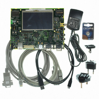
KIT EVAL FOR AT91SAM9G45
Manufacturer
Atmel
Series
AT91SAM Smart ARMr
Type
MCUr
Datasheets
1.AT91SAM9G45-EKES.pdf
(56 pages)
2.AT91SAM9G45-EKES.pdf
(1218 pages)
3.AT91SAM9G45-EKES.pdf
(66 pages)
Specifications of AT91SAM9G45-EKES
Contents
Board
Processor To Be Evaluated
SAM9G45
Data Bus Width
32 bit
Interface Type
I2C, SPI, UART
Maximum Operating Temperature
+ 50 C
Minimum Operating Temperature
- 10 C
Operating Supply Voltage
1.8 V to 3.3 V
For Use With/related Products
AT91SAM9G45
Lead Free Status / RoHS Status
Lead free / RoHS Compliant
Other names
Q4626953


• BAT: Byte Access Type
This field is used only if DBW defines a 16- or 32-bit data bus.
• DBW: Data Bus Width
• TDF_CYCLES: Data Float Time
This field gives the integer number of clock cycles required by the external device to release the data after the rising edge
of the read controlling signal. The SMC always provide one full cycle of bus turnaround after the TDF_CYCLES period. The
external bus cannot be used by another chip select during TDF_CYCLES + 1 cycles. From 0 up to 15 TDF_CYCLES can
be set.
• TDF_MODE: TDF Optimization
1: TDF optimization is enabled.
0: TDF optimization is disabled.
• PMEN: Page Mode Enabled
1: Asynchronous burst read in page mode is applied on the corresponding chip select.
0: Standard read is applied.
• PS: Page Size
If page mode is enabled, this field indicates the size of the page in bytes.
6438F–ATARM–21-Jun-10
• Ready Mode: The NWAIT signal indicates the availability of the external device at the end of the pulse of the controlling
• 1: Byte write access type:
• 0: Byte select access type:
read or write signal, to complete the access. If high, the access normally completes. If low, the access is extended until
NWAIT returns high.
– Write operation is controlled using NCS, NWR0, NWR1, NWR2, NWR3.
– Read operation is controlled using NCS and NRD.
– Write operation is controlled using NCS, NWE, NBS0, NBS1, NBS2 and NBS3
– Read operation is controlled using NCS, NRD, NBS0, NBS1, NBS2 and NBS3
– The number of TDF wait states is optimized using the setup period of the next read/write access.
– The number of TDF wait states is inserted before the next access begins.
0
0
1
1
0
0
1
1
DBW
PS
0
1
0
1
0
1
0
1
Data Bus Width
8-bit bus
16-bit bus
32-bit bus
Reserved
Page Size
4-byte page
8-byte page
16-byte page
32-byte page
AT91SAM9G45
227
Related parts for AT91SAM9G45-EKES
Image
Part Number
Description
Manufacturer
Datasheet
Request
R

Part Number:
Description:
MCU ARM9 64K SRAM 144-LFBGA
Manufacturer:
Atmel
Datasheet:

Part Number:
Description:
IC ARM7 MCU FLASH 256K 100LQFP
Manufacturer:
Atmel
Datasheet:

Part Number:
Description:
IC ARM9 MPU 217-LFBGA
Manufacturer:
Atmel
Datasheet:
Part Number:
Description:
MCU ARM9 ULTRA LOW PWR 217-LFBGA
Manufacturer:
Atmel
Datasheet:

Part Number:
Description:
MCU ARM9 324-TFBGA
Manufacturer:
Atmel
Datasheet:
Part Number:
Description:
IC MCU ARM9 SAMPLING 217CBGA
Manufacturer:
Atmel
Datasheet:
Part Number:
Description:
IC ARM9 MCU 217-LFBGA
Manufacturer:
Atmel
Datasheet:

Part Number:
Description:
IC ARM9 MCU 208-PQFP
Manufacturer:
Atmel
Datasheet:
Part Number:
Description:
MCU ARM 512K HS FLASH 100-LQFP
Manufacturer:
Atmel
Datasheet:

Part Number:
Description:
MCU ARM 512K HS FLASH 100-TFBGA
Manufacturer:
Atmel
Datasheet:
Part Number:
Description:
IC ARM9 MCU 200 MHZ 324-TFBGA
Manufacturer:
Atmel
Datasheet:

Part Number:
Description:
IC ARM MCU 16BIT 128K 256BGA
Manufacturer:
Atmel
Datasheet:

Part Number:
Description:
IC ARM7 MCU 32BIT 128K 64LQFP
Manufacturer:
Atmel
Datasheet:

Part Number:
Description:
IC ARM7 MCU FLASH 256K 128-LQFP
Manufacturer:
Atmel
Datasheet:
Part Number:
Description:
IC ARM7 MCU FLASH 512K 128-LQFP
Manufacturer:
Atmel
Datasheet: