AT91SAM9G45-EKES Atmel, AT91SAM9G45-EKES Datasheet - Page 232
AT91SAM9G45-EKES
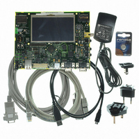
Manufacturer Part Number
AT91SAM9G45-EKES
Description
KIT EVAL FOR AT91SAM9G45
Manufacturer
Atmel
Series
AT91SAM Smart ARMr
Type
MCUr
Datasheets
1.AT91SAM9G45-EKES.pdf
(56 pages)
2.AT91SAM9G45-EKES.pdf
(1218 pages)
3.AT91SAM9G45-EKES.pdf
(66 pages)
Specifications of AT91SAM9G45-EKES
Contents
Board
Processor To Be Evaluated
SAM9G45
Data Bus Width
32 bit
Interface Type
I2C, SPI, UART
Maximum Operating Temperature
+ 50 C
Minimum Operating Temperature
- 10 C
Operating Supply Voltage
1.8 V to 3.3 V
For Use With/related Products
AT91SAM9G45
Lead Free Status / RoHS Status
Lead free / RoHS Compliant
Other names
Q4626953


22.3.2
232
AT91SAM9G45
Low-power DDR1-SDRAM Initialization
After initialization, the SDR-SDRAM device is fully functional.
The initialization sequence is generated by software. The low-power DDR1-SDRAM devices are
initialized by the following sequence:
A minimum pause of 200 μs will be provided to precede any signal toggle.
Note:
10. Write the refresh rate into the count field in the DDRSDRC Refresh Timer register (see
1. Program the memory device type into the Memory Device Register (see
2. Program the features of the low-power DDR1-SDRAM device into the Configuration
3. Program temperature compensated self refresh (tcr), Partial array self refresh (pasr)
4. An NOP command will be issued to the low-power DDR1-SDRAM. Program NOP com-
5. An all banks precharge command is issued to the low-power DDR1-SDRAM. Program
6. Two auto-refresh (CBR) cycles are provided. Program the auto refresh command
7. An Extended Mode Register set (EMRS) cycle is issued to program the low-power
8. A Mode Register set (MRS) cycle is issued to program the parameters of the low-power
page
requires a refresh every 15.625 μs or 7.81 μs. With a 100 MHz frequency, the refresh
timer count register must to be set with (15.625 /100 MHz) = 1562 i.e. 0x061A or (7.81
/100 MHz) = 781 i.e. 0x030d
on page
Register: asynchronous timing (trc, tras, etc.), number of columns, rows, banks, cas
latency. See
22.7.5 on page
and Drive strength (ds) into the Low-power Register. See
mand into the Mode Register, the application must set Mode to 1 in the Mode Register
(see
address to acknowledge this command. Now clocks which drive DDR1-SDRAM device
are enabled.
all banks precharge command into the Mode Register, the application must set Mode to
2 in the Mode Register (See
any low-power DDR1-SDRAM address to acknowledge this command
(CBR) into the Mode Register, the application must set Mode to 4 in the Mode Register
(see
SDRAM location twice to acknowledge these commands.
DDR1-SDRAM parameters (TCSR, PASR, DS). The application must set Mode to 5 in
the Mode Register (see
SDRAM to acknowledge this command. The write address must be chosen so that
BA[1] is set to 1 BA[0] is set to 0. For example, with a 16-bit 128 MB SDRAM (12 rows,
9 columns, 4 banks) bank address, the low-power DDR1-SDRAM write access should
be done at the address 0x20800000.
DDR1-SDRAM devices, in particular CAS latency, burst length. The application must
set Mode to 3 in the Mode Register (see
write access to the low-power DDR1-SDRAM to acknowledge this command. The write
address must be chosen so that BA[1:0] bits are set to 0. For example, with a 16-bit 128
MB low-power DDR1-SDRAM (12 rows, 9 columns, 4 banks) bank address, the
SDRAM write access should be done at the address 0x20000000
This address is for example purposes only. The real address is dependent on implementation in
the product.
Section 22.7.1 on page
Section 22.7.1 on page
261). (Refresh rate = delay between refresh cycles). The SDR-SDRAM device
271).
Section 22.7.3 on page
267.
Section 22.7.1 on page
Section 22.7.1 on page
260). Perform a write access to any DDR1-SDRAM
260). Perform a write access to any low-power DDR1-
262,
Section 22.7.1 on page
Section 22.7.4 on page 265
260) and perform a write access to the
260). Perform a write access to
Section 22.7.7 on page
260) and perform a
and
6438F–ATARM–21-Jun-10
Section 22.7.8
Section
269.
Related parts for AT91SAM9G45-EKES
Image
Part Number
Description
Manufacturer
Datasheet
Request
R

Part Number:
Description:
MCU ARM9 64K SRAM 144-LFBGA
Manufacturer:
Atmel
Datasheet:

Part Number:
Description:
IC ARM7 MCU FLASH 256K 100LQFP
Manufacturer:
Atmel
Datasheet:

Part Number:
Description:
IC ARM9 MPU 217-LFBGA
Manufacturer:
Atmel
Datasheet:
Part Number:
Description:
MCU ARM9 ULTRA LOW PWR 217-LFBGA
Manufacturer:
Atmel
Datasheet:

Part Number:
Description:
MCU ARM9 324-TFBGA
Manufacturer:
Atmel
Datasheet:
Part Number:
Description:
IC MCU ARM9 SAMPLING 217CBGA
Manufacturer:
Atmel
Datasheet:
Part Number:
Description:
IC ARM9 MCU 217-LFBGA
Manufacturer:
Atmel
Datasheet:

Part Number:
Description:
IC ARM9 MCU 208-PQFP
Manufacturer:
Atmel
Datasheet:
Part Number:
Description:
MCU ARM 512K HS FLASH 100-LQFP
Manufacturer:
Atmel
Datasheet:

Part Number:
Description:
MCU ARM 512K HS FLASH 100-TFBGA
Manufacturer:
Atmel
Datasheet:
Part Number:
Description:
IC ARM9 MCU 200 MHZ 324-TFBGA
Manufacturer:
Atmel
Datasheet:

Part Number:
Description:
IC ARM MCU 16BIT 128K 256BGA
Manufacturer:
Atmel
Datasheet:

Part Number:
Description:
IC ARM7 MCU 32BIT 128K 64LQFP
Manufacturer:
Atmel
Datasheet:

Part Number:
Description:
IC ARM7 MCU FLASH 256K 128-LQFP
Manufacturer:
Atmel
Datasheet:
Part Number:
Description:
IC ARM7 MCU FLASH 512K 128-LQFP
Manufacturer:
Atmel
Datasheet: