AT91SAM9G45-EKES Atmel, AT91SAM9G45-EKES Datasheet - Page 169
AT91SAM9G45-EKES
Manufacturer Part Number
AT91SAM9G45-EKES
Description
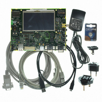
KIT EVAL FOR AT91SAM9G45
Manufacturer
Atmel
Series
AT91SAM Smart ARMr
Type
MCUr
Datasheets
1.AT91SAM9G45-EKES.pdf
(56 pages)
2.AT91SAM9G45-EKES.pdf
(1218 pages)
3.AT91SAM9G45-EKES.pdf
(66 pages)
Specifications of AT91SAM9G45-EKES
Contents
Board
Processor To Be Evaluated
SAM9G45
Data Bus Width
32 bit
Interface Type
I2C, SPI, UART
Maximum Operating Temperature
+ 50 C
Minimum Operating Temperature
- 10 C
Operating Supply Voltage
1.8 V to 3.3 V
For Use With/related Products
AT91SAM9G45
Lead Free Status / RoHS Status
Lead free / RoHS Compliant
Other names
Q4626953


Table 20-7.
6438F–ATARM–21-Jun-10
Mode
Attribute Memory
Common Memory
I/O Mode
Alternate True IDE Mode
Standby Mode or
Address Space is not
assigned to CF
Alternate Status Read
CFCE1 and CFCE2 Signals
Read/Write Signals
Control Register
Drive Address
Data Register
Task File
CFCE1 and CFCE2 Truth Table
To cover all types of access, the SMC must be alternatively set to drive 8-bit data bus or 16-bit
data bus. The odd byte access on the D[7:0] bus is only possible when the SMC is configured to
drive 8-bit memory devices on the corresponding NCS pin (NCS4 or NCS5). The Chip Select
Register (DBW field in the corresponding Chip Select Register) of the NCS4 and/or NCS5
address space must be set as shown in
NBS1 and NBS0 are the byte selection signals from SMC and are available when the SMC is set
in Byte Select mode on the corresponding Chip Select.
The CFCE1 and CFCE2 waveforms are identical to the corresponding NCSx waveform. For
details on these waveforms and timings, refer to the Static Memory Controller section.
In I/O mode and True IDE mode, the CompactFlash logic drives the read and write command
signals of the SMC on CFIOR and CFIOW signals, while the CFOE and CFWE signals are deac-
tivated. Likewise, in common memory mode and attribute memory mode, the SMC signals are
driven on the CFOE and CFWE signals, while the CFIOR and CFIOW are deactivated.
20-6 on page 170
Attribute memory mode, common memory mode and I/O mode are supported by setting the
address setup and hold time on the NCS4 (and/or NCS5) chip select to the appropriate values.
For details on these signal waveforms, please refer to the section: Setup and Hold Cycles of the
Static Memory Controller section.
CFCE2
NBS1
NBS1
NBS1
1
1
1
1
0
0
1
CFCE1
demonstrates a schematic representation of this logic.
NBS0
NBS0
NBS0
0
0
0
0
1
1
1
True IDE Mode
16 bits
16 bits
16 bits
16bits
DBW
8 bits
8 bits
8 bits
8 bits
Don’t
Care
–
Table 20-7
Access to Even Byte on D[7:0]
Access to Odd Byte on D[15:8]
Access to Even Byte on D[7:0]
Access to Odd Byte on D[15:8]
Access to Even Byte on D[7:0]
Access to Odd Byte on D[7:0]
Access to Even Byte on D[7:0]
Access to Odd Byte on D[15:8]
Access to Even Byte on D[7:0]
Comment
Access to Even Byte on D[7:0]
Access to Odd Byte on D[7:0]
Access to Odd Byte on D[7:0]
Access to Odd Byte on D[7:0]
to enable the required access type.
–
AT91SAM9G45
SMC Access Mode
Byte Select
Byte Select
Byte Select
Byte Select
Don’t Care
–
Figure
169
Related parts for AT91SAM9G45-EKES
Image
Part Number
Description
Manufacturer
Datasheet
Request
R

Part Number:
Description:
MCU ARM9 64K SRAM 144-LFBGA
Manufacturer:
Atmel
Datasheet:

Part Number:
Description:
IC ARM7 MCU FLASH 256K 100LQFP
Manufacturer:
Atmel
Datasheet:

Part Number:
Description:
IC ARM9 MPU 217-LFBGA
Manufacturer:
Atmel
Datasheet:
Part Number:
Description:
MCU ARM9 ULTRA LOW PWR 217-LFBGA
Manufacturer:
Atmel
Datasheet:

Part Number:
Description:
MCU ARM9 324-TFBGA
Manufacturer:
Atmel
Datasheet:
Part Number:
Description:
IC MCU ARM9 SAMPLING 217CBGA
Manufacturer:
Atmel
Datasheet:
Part Number:
Description:
IC ARM9 MCU 217-LFBGA
Manufacturer:
Atmel
Datasheet:

Part Number:
Description:
IC ARM9 MCU 208-PQFP
Manufacturer:
Atmel
Datasheet:
Part Number:
Description:
MCU ARM 512K HS FLASH 100-LQFP
Manufacturer:
Atmel
Datasheet:

Part Number:
Description:
MCU ARM 512K HS FLASH 100-TFBGA
Manufacturer:
Atmel
Datasheet:
Part Number:
Description:
IC ARM9 MCU 200 MHZ 324-TFBGA
Manufacturer:
Atmel
Datasheet:

Part Number:
Description:
IC ARM MCU 16BIT 128K 256BGA
Manufacturer:
Atmel
Datasheet:

Part Number:
Description:
IC ARM7 MCU 32BIT 128K 64LQFP
Manufacturer:
Atmel
Datasheet:

Part Number:
Description:
IC ARM7 MCU FLASH 256K 128-LQFP
Manufacturer:
Atmel
Datasheet:
Part Number:
Description:
IC ARM7 MCU FLASH 512K 128-LQFP
Manufacturer:
Atmel
Datasheet: