AT91SAM9G45-EKES Atmel, AT91SAM9G45-EKES Datasheet - Page 461
AT91SAM9G45-EKES
Manufacturer Part Number
AT91SAM9G45-EKES
Description
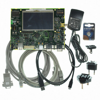
KIT EVAL FOR AT91SAM9G45
Manufacturer
Atmel
Series
AT91SAM Smart ARMr
Type
MCUr
Datasheets
1.AT91SAM9G45-EKES.pdf
(56 pages)
2.AT91SAM9G45-EKES.pdf
(1218 pages)
3.AT91SAM9G45-EKES.pdf
(66 pages)
Specifications of AT91SAM9G45-EKES
Contents
Board
Processor To Be Evaluated
SAM9G45
Data Bus Width
32 bit
Interface Type
I2C, SPI, UART
Maximum Operating Temperature
+ 50 C
Minimum Operating Temperature
- 10 C
Operating Supply Voltage
1.8 V to 3.3 V
For Use With/related Products
AT91SAM9G45
Lead Free Status / RoHS Status
Lead free / RoHS Compliant
Other names
Q4626953


30.4.12
6438F–ATARM–21-Jun-10
Programmable I/O Delays
If a write access in a write-protected register is detected, then the WPVS flag in the PIO Write
Protect Status Register (PIO_WPSR) is set and the field WPVSRC indicates in which register
the write access has been attempted.
The WPVS flag is automatically reset after reading the PIO Write Protect Status Register
(PIO_WPSR).
List of the write-protected registers:
The PIO interface consists of a series of signals driven by peripherals or directly by sofware. The
simultaneous switching outputs on these busses may lead to a peak of current in the internal
and external power supply lines.
In order to reduce the peak of current in such cases, additional propagation delays can be
adjusted independently for pad buffers by means of configuration registers, PIO_DELAY.
For each I/O, the additional programmable delays range from 0 to 4 ns (Worst Case PVT). The
delay can differ between IOs supporting this feature. The delay can be modified according to
programming for each I/O. The minimum additional delay that can be programmed on a PAD
supporting this feature is 1/16 of the maximum programmable delay.
Only PADs PC[12], PC[7:2], PA[30:23] and PA[9:2] can be configured.
When programming 0x0 in fields, no delay is added (reset value) and the propagation delay of
the pad buffers is the inherent delay of the pad buffer. When programming 0xF in field, the prop-
agation delay of the corresponding pad is maximal.
•
•
•
•
•
•
•
•
•
•
•
•
•
•
•
•
“PIO Enable Register” on page 466
“PIO Disable Register” on page 466
“PIO Output Enable Register” on page 467
“PIO Output Disable Register” on page 468
“PIO Input Filter Enable Register” on page 469
“PIO Input Filter Disable Register” on page 469
“PIO Set Output Data Register” on page 470
“PIO Clear Output Data Register” on page 471
“PIO Multi-driver Enable Register” on page 474
“PIO Multi-driver Disable Register” on page 475
“PIO Pull Up Disable Register” on page 476
“PIO Pull Up Enable Register” on page 476
“PIO Peripheral A Select Register” on page 477
“PIO Peripheral B Select Register” on page 478
“PIO Output Write Enable Register” on page 479
“PIO Output Write Disable Register” on page 479
AT91SAM9G45
461
Related parts for AT91SAM9G45-EKES
Image
Part Number
Description
Manufacturer
Datasheet
Request
R

Part Number:
Description:
MCU ARM9 64K SRAM 144-LFBGA
Manufacturer:
Atmel
Datasheet:

Part Number:
Description:
IC ARM7 MCU FLASH 256K 100LQFP
Manufacturer:
Atmel
Datasheet:

Part Number:
Description:
IC ARM9 MPU 217-LFBGA
Manufacturer:
Atmel
Datasheet:
Part Number:
Description:
MCU ARM9 ULTRA LOW PWR 217-LFBGA
Manufacturer:
Atmel
Datasheet:

Part Number:
Description:
MCU ARM9 324-TFBGA
Manufacturer:
Atmel
Datasheet:
Part Number:
Description:
IC MCU ARM9 SAMPLING 217CBGA
Manufacturer:
Atmel
Datasheet:
Part Number:
Description:
IC ARM9 MCU 217-LFBGA
Manufacturer:
Atmel
Datasheet:

Part Number:
Description:
IC ARM9 MCU 208-PQFP
Manufacturer:
Atmel
Datasheet:
Part Number:
Description:
MCU ARM 512K HS FLASH 100-LQFP
Manufacturer:
Atmel
Datasheet:

Part Number:
Description:
MCU ARM 512K HS FLASH 100-TFBGA
Manufacturer:
Atmel
Datasheet:
Part Number:
Description:
IC ARM9 MCU 200 MHZ 324-TFBGA
Manufacturer:
Atmel
Datasheet:

Part Number:
Description:
IC ARM MCU 16BIT 128K 256BGA
Manufacturer:
Atmel
Datasheet:

Part Number:
Description:
IC ARM7 MCU 32BIT 128K 64LQFP
Manufacturer:
Atmel
Datasheet:

Part Number:
Description:
IC ARM7 MCU FLASH 256K 128-LQFP
Manufacturer:
Atmel
Datasheet:
Part Number:
Description:
IC ARM7 MCU FLASH 512K 128-LQFP
Manufacturer:
Atmel
Datasheet: