OM13006,598 NXP Semiconductors, OM13006,598 Datasheet - Page 99
OM13006,598
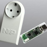
Manufacturer Part Number
OM13006,598
Description
BOARD EVAL EM773 METER EU PLUG
Manufacturer
NXP Semiconductors
Type
Other Power Managementr
Specifications of OM13006,598
Design Resources
Plug Meter Schematics, Gerber Files USB Dongle Schematics, Gerber Files
Main Purpose
Power Management, Energy/Power Meter
Embedded
Yes, MCU, 32-Bit
Utilized Ic / Part
EM773FHN33,551
Interface Type
USB
Maximum Operating Temperature
+ 150 C
Operating Supply Voltage
1.8 V to 3.6 V
Product
Power Management Development Tools
Lead Free Status / RoHS Status
Lead free / RoHS Compliant
Primary Attributes
-
Secondary Attributes
-
Lead Free Status / Rohs Status
Lead free / RoHS Compliant
For Use With/related Products
EM773, OL2381
Other names
568-6681


NXP Semiconductors
10.6 Pin description
10.7 Clocking and power control
10.8 Register description
Table 112. Register overview: I
UM10415
User manual
Name
I2C0CONSET R/W
I2C0STAT
I2C0DAT
I2C0ADR0
I2C0SCLH
I2C0SCLL
I2C0CONCLR WO
I2C0MMCTRL R/W
Access Address
RO
R/W
R/W
R/W
R/W
Table 111. I
The I
IOCON_PIO0_5
Fast-mode Plus, rates above 400 kHz and up to 1 MHz may be selected. The I
are open-drain outputs and fully compatible with the I
The clock to the I
Figure
(Table
Remark: Before accessing the I2C block, ensure that the I2C_RST_N bit (bit 1) in the
PRESETCTRL register
block.
Pin
SDA
SCL
offset
0x000
0x004
0x008
0x00C
0x010
0x014
0x018
0x01C
2
C-bus pins must be configured through the IOCON_PIO0_4
17) for power savings.
3). This clock can be disabled through bit 5 in the AHBCLKCTRL register
2
C (base address 0x4000 0000)
2
C-bus pin description
Description
I2C Control Set Register. When a one is written to a bit of this register,
the corresponding bit in the I
no effect on the corresponding bit in the I
I2C Status Register. During I
status codes that allow software to determine the next action needed.
I2C Data Register. During master or slave transmit mode, data to be
transmitted is written to this register. During master or slave receive
mode, data that has been received may be read from this register.
I2C Slave Address Register 0. Contains the 7-bit slave address for
operation of the I
mode. The least significant bit determines whether a slave responds to
the General Call address.
SCH Duty Cycle Register High Half Word. Determines the high time of
the I
SCL Duty Cycle Register Low Half Word. Determines the low time of
the I
frequency generated by an I
mode.
I2C Control Clear Register. When a one is written to a bit of this register,
the corresponding bit in the I
has no effect on the corresponding bit in the I
Monitor mode control register.
Type
Input/Output
Input/Output
All information provided in this document is subject to legal disclaimers.
(Table
2
2
2
C-bus interface (PCLK_I2C) is provided by the system clock (see
C clock.
C clock. I2nSCLL and I2nSCLH together determine the clock
Rev. 1 — 10 September 2010
56) registers for Standard/ Fast-mode or Fast-mode Plus. In
(Table
2
C interface in slave mode, and is not used in master
5) is set to 1. This de-asserts the reset signal to the I2C
Description
I
I
2
2
C Serial Data
C Serial Clock
2
2
2
C master and certain times used in slave
C control register is set. Writing a zero has
C control register is cleared. Writing a zero
2
C operation, this register provides detailed
Chapter 10: EM773 I2C-bus interface
2
C control register.
2
C-bus specification.
2
C control register.
(Table
UM10415
© NXP B.V. 2010. All rights reserved.
55) and
2
C-bus pins
Reset
value
0x00
0xF8
0x00
0x00
0x04
0x04
NA
0x00
99 of 310
[1]
Related parts for OM13006,598
Image
Part Number
Description
Manufacturer
Datasheet
Request
R

Part Number:
Description:
NXP Semiconductors designed the LPC2420/2460 microcontroller around a 16-bit/32-bitARM7TDMI-S CPU core with real-time debug interfaces that include both JTAG andembedded trace
Manufacturer:
NXP Semiconductors
Datasheet:

Part Number:
Description:
NXP Semiconductors designed the LPC2458 microcontroller around a 16-bit/32-bitARM7TDMI-S CPU core with real-time debug interfaces that include both JTAG andembedded trace
Manufacturer:
NXP Semiconductors
Datasheet:
Part Number:
Description:
NXP Semiconductors designed the LPC2468 microcontroller around a 16-bit/32-bitARM7TDMI-S CPU core with real-time debug interfaces that include both JTAG andembedded trace
Manufacturer:
NXP Semiconductors
Datasheet:
Part Number:
Description:
NXP Semiconductors designed the LPC2470 microcontroller, powered by theARM7TDMI-S core, to be a highly integrated microcontroller for a wide range ofapplications that require advanced communications and high quality graphic displays
Manufacturer:
NXP Semiconductors
Datasheet:
Part Number:
Description:
NXP Semiconductors designed the LPC2478 microcontroller, powered by theARM7TDMI-S core, to be a highly integrated microcontroller for a wide range ofapplications that require advanced communications and high quality graphic displays
Manufacturer:
NXP Semiconductors
Datasheet:
Part Number:
Description:
The Philips Semiconductors XA (eXtended Architecture) family of 16-bit single-chip microcontrollers is powerful enough to easily handle the requirements of high performance embedded applications, yet inexpensive enough to compete in the market for hi
Manufacturer:
NXP Semiconductors
Datasheet:
Part Number:
Description:
The XA-S3 device is a member of Philips Semiconductors? XA(eXtended Architecture) family of high performance 16-bitsingle-chip microcontrollers
Manufacturer:
NXP Semiconductors
Datasheet:

Part Number:
Description:
The NXP BlueStreak LH75401/LH75411 family consists of two low-cost 16/32-bit System-on-Chip (SoC) devices
Manufacturer:
NXP Semiconductors
Datasheet:
Part Number:
Description:
The NXP LPC3130/3131 combine an 180 MHz ARM926EJ-S CPU core, high-speed USB2
Manufacturer:
NXP Semiconductors
Datasheet:
Part Number:
Description:
The NXP LPC3141 combine a 270 MHz ARM926EJ-S CPU core, High-speed USB 2
Manufacturer:
NXP Semiconductors
Part Number:
Description:
The NXP LPC3143 combine a 270 MHz ARM926EJ-S CPU core, High-speed USB 2
Manufacturer:
NXP Semiconductors

Part Number:
Description:
The NXP LPC3152 combines an 180 MHz ARM926EJ-S CPU core, High-speed USB 2
Manufacturer:
NXP Semiconductors
Part Number:
Description:
The NXP LPC3154 combines an 180 MHz ARM926EJ-S CPU core, High-speed USB 2
Manufacturer:
NXP Semiconductors

Part Number:
Description:
Standard level N-channel enhancement mode Field-Effect Transistor (FET) in a plastic package using NXP High-Performance Automotive (HPA) TrenchMOS technology
Manufacturer:
NXP Semiconductors
Datasheet: