OM13006,598 NXP Semiconductors, OM13006,598 Datasheet - Page 257
OM13006,598
Manufacturer Part Number
OM13006,598
Description
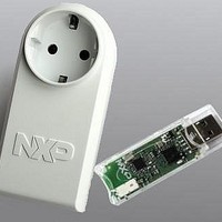
BOARD EVAL EM773 METER EU PLUG
Manufacturer
NXP Semiconductors
Type
Other Power Managementr
Specifications of OM13006,598
Design Resources
Plug Meter Schematics, Gerber Files USB Dongle Schematics, Gerber Files
Main Purpose
Power Management, Energy/Power Meter
Embedded
Yes, MCU, 32-Bit
Utilized Ic / Part
EM773FHN33,551
Interface Type
USB
Maximum Operating Temperature
+ 150 C
Operating Supply Voltage
1.8 V to 3.6 V
Product
Power Management Development Tools
Lead Free Status / RoHS Status
Lead free / RoHS Compliant
Primary Attributes
-
Secondary Attributes
-
Lead Free Status / Rohs Status
Lead free / RoHS Compliant
For Use With/related Products
EM773, OL2381
Other names
568-6681


NXP Semiconductors
UM10415
User manual
20.4.4.4.5 Examples
20.4.4.5.1 Syntax
20.4.4.5.2 Operation
20.4.4.5.3 Restrictions
20.4.4.5 LDM and STM
Load and Store Multiple registers.
LDM Rn{!}, reglist
STM Rn!, reglist
where:
LDMIA and LDMFD are synonyms for LDM. LDMIA refers to the base register being
Incremented After each access. LDMFD refers to its use for popping data from Full
Descending stacks.
STMIA and STMEA are synonyms for STM. STMIA refers to the base register being
Incremented After each access. STMEA refers to its use for pushing data onto Empty
Ascending stacks.
LDM instructions load the registers in reglist with word values from memory addresses
based on Rn.
STM instructions store the word values in the registers in reglist to memory addresses
based on Rn.
The memory addresses used for the accesses are at 4-byte intervals ranging from the
value in the register specified by Rn to the value in the register specified by Rn + 4 * (n-1),
where n is the number of registers in reglist. The accesses happens in order of increasing
register numbers, with the lowest numbered register using the lowest memory address
and the highest number register using the highest memory address. If the writeback suffix
is specified, the value in the register specified by Rn + 4 *n is written back to the register
specified by Rn.
In these instructions:
•
•
Rn is the register on which the memory addresses are based.
! writeback suffix.
reglist is a list of one or more registers to be loaded or stored, enclosed in braces. It can
contain register ranges. It must be comma separated if it contains more than one
register or register range, see
LDR
LDR
reglist and Rn are limited to R0-R7.
the writeback suffix must always be used unless the instruction is an LDM where
reglist also contains Rn, in which case the writeback suffix must not be used.
R0, LookUpTable
R3, [PC, #100]
All information provided in this document is subject to legal disclaimers.
Rev. 1 — 10 September 2010
Chapter 20: Appendix EM773 ARM Cortex-M0 reference
; Load R0 with a word of data from an address
; Load R3 with memory word at (PC + 100).
Section
; labelled as LookUpTable.
20–20.4.4.5.5.
UM10415
© NXP B.V. 2010. All rights reserved.
257 of 310
Related parts for OM13006,598
Image
Part Number
Description
Manufacturer
Datasheet
Request
R

Part Number:
Description:
NXP Semiconductors designed the LPC2420/2460 microcontroller around a 16-bit/32-bitARM7TDMI-S CPU core with real-time debug interfaces that include both JTAG andembedded trace
Manufacturer:
NXP Semiconductors
Datasheet:

Part Number:
Description:
NXP Semiconductors designed the LPC2458 microcontroller around a 16-bit/32-bitARM7TDMI-S CPU core with real-time debug interfaces that include both JTAG andembedded trace
Manufacturer:
NXP Semiconductors
Datasheet:
Part Number:
Description:
NXP Semiconductors designed the LPC2468 microcontroller around a 16-bit/32-bitARM7TDMI-S CPU core with real-time debug interfaces that include both JTAG andembedded trace
Manufacturer:
NXP Semiconductors
Datasheet:
Part Number:
Description:
NXP Semiconductors designed the LPC2470 microcontroller, powered by theARM7TDMI-S core, to be a highly integrated microcontroller for a wide range ofapplications that require advanced communications and high quality graphic displays
Manufacturer:
NXP Semiconductors
Datasheet:
Part Number:
Description:
NXP Semiconductors designed the LPC2478 microcontroller, powered by theARM7TDMI-S core, to be a highly integrated microcontroller for a wide range ofapplications that require advanced communications and high quality graphic displays
Manufacturer:
NXP Semiconductors
Datasheet:
Part Number:
Description:
The Philips Semiconductors XA (eXtended Architecture) family of 16-bit single-chip microcontrollers is powerful enough to easily handle the requirements of high performance embedded applications, yet inexpensive enough to compete in the market for hi
Manufacturer:
NXP Semiconductors
Datasheet:
Part Number:
Description:
The XA-S3 device is a member of Philips Semiconductors? XA(eXtended Architecture) family of high performance 16-bitsingle-chip microcontrollers
Manufacturer:
NXP Semiconductors
Datasheet:

Part Number:
Description:
The NXP BlueStreak LH75401/LH75411 family consists of two low-cost 16/32-bit System-on-Chip (SoC) devices
Manufacturer:
NXP Semiconductors
Datasheet:
Part Number:
Description:
The NXP LPC3130/3131 combine an 180 MHz ARM926EJ-S CPU core, high-speed USB2
Manufacturer:
NXP Semiconductors
Datasheet:
Part Number:
Description:
The NXP LPC3141 combine a 270 MHz ARM926EJ-S CPU core, High-speed USB 2
Manufacturer:
NXP Semiconductors
Part Number:
Description:
The NXP LPC3143 combine a 270 MHz ARM926EJ-S CPU core, High-speed USB 2
Manufacturer:
NXP Semiconductors

Part Number:
Description:
The NXP LPC3152 combines an 180 MHz ARM926EJ-S CPU core, High-speed USB 2
Manufacturer:
NXP Semiconductors
Part Number:
Description:
The NXP LPC3154 combines an 180 MHz ARM926EJ-S CPU core, High-speed USB 2
Manufacturer:
NXP Semiconductors

Part Number:
Description:
Standard level N-channel enhancement mode Field-Effect Transistor (FET) in a plastic package using NXP High-Performance Automotive (HPA) TrenchMOS technology
Manufacturer:
NXP Semiconductors
Datasheet: