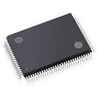
LFXP3C-3TN100I Lattice, LFXP3C-3TN100I Datasheet - Page 378

LFXP3C-3TN100I
Manufacturer Part Number
LFXP3C-3TN100I
Description
FPGA - Field Programmable Gate Array 3.1K LUTs 62 IO 1.8/ 2.5/3.3V -3 Spd I
Manufacturer
Lattice
Specifications of LFXP3C-3TN100I
Number Of Programmable I/os
62
Data Ram Size
55296
Supply Voltage (max)
3.465 V
Maximum Operating Temperature
+ 100 C
Minimum Operating Temperature
- 40 C
Mounting Style
SMD/SMT
Supply Voltage (min)
1.71 V
Package / Case
TQFP-100
Package
100TQFP
Family Name
LatticeXP
Device Logic Units
3000
Maximum Internal Frequency
320 MHz
Typical Operating Supply Voltage
1.8|2.5|3.3 V
Maximum Number Of User I/os
62
Ram Bits
55296
Re-programmability Support
Yes
Lead Free Status / RoHS Status
Lead free / RoHS Compliant
Available stocks
Company
Part Number
Manufacturer
Quantity
Price
Company:
Part Number:
LFXP3C-3TN100I
Manufacturer:
Lattice Semiconductor Corporation
Quantity:
10 000
- Current page: 378 of 397
- Download datasheet (10Mb)
Lattice Semiconductor
Figure 14-1. BGA Breakout Routing Terms
Lattice provides BGA breakout and routing examples for various fine pitch packages
port/pcbdesignsupport/bgabreakoutroutingexample/index.cfm). Each package example is built to comply with
IPC7351 (www.ipc.org) specifications and nomenclature conventions. Some examples include different layout
options depending on design and cost goals. For example, the 256-ball chip array BGA (BN256) examples demon-
strate a design with fully-utilized I/Os, fine trace width and pitch, on a 6-layer PCB stack-up and a less expensive
design with relaxed design rules, and fewer I/O pads routed, on a 4-layer PCB stack up.
Table 14-3. Package Layout Example Summary
For mechanical dimension details on packages, see the Lattice
In order to show how some of the routing challenges are solved, examples are provided for fine-pitch BGA pack-
ages from the MachXO™ and the ispMACH
packaged products.
Package
UMN64
MN100
MN132
MN144
BN256
MN64
Example #
1
1
2
1
2
1
2
1
2
1
Pitch (mm)
0.5
0.4
0.5
0.5
0.5
0.5
0.5
0.5
0.8
0.8
Signal/
Layers
Power
6
6
4
4
4
4
6
4
6
4
®
4000ZE families. Principles for these apply to other Lattice BGA
Space (mm)
.100/.100
.100/.100
.085/.085
.100/.100
.085/.085
.100/.100
.100/.100
.100/.100
.100/.100
.100/.100
Width-
Trace/
14-3
Package Diagrams
Ball Pad
(mm)
.23
.18
.23
.23
.23
.23
.23
.23
.35
.35
PCB Layout Recommendations
Ball Mask
(mm)
.33
.28
.38
.38
.38
.38
.33
.38
.50
.50
document.
(www.latticesemi.com/sup-
for BGA Packages
Via Pad
(mm)
.30
.25
.45
.45
.40
.40
.30
.30
.40
.40
Via Drill
(mm)
.125
.125
.125
.125
.10
.20
.20
.15
.15
.15
Related parts for LFXP3C-3TN100I
Image
Part Number
Description
Manufacturer
Datasheet
Request
R

Part Number:
Description:
FPGA - Field Programmable Gate Array 3.1K LUTs 136 IO 1.8 /2.5/3.3V -3 Spd I
Manufacturer:
Lattice

Part Number:
Description:
FPGA - Field Programmable Gate Array 3.1K LUTs 62 IO 1.8/ 2.5/3.3V -3 Spd I
Manufacturer:
Lattice

Part Number:
Description:
FPGA - Field Programmable Gate Array 3.1K LUTs 136 IO 1.8 /2.5/3.3V -3 Spd
Manufacturer:
Lattice

Part Number:
Description:
FPGA - Field Programmable Gate Array 3.1K LUTs 100 I/O 1.8/2.5/3.3V -3 Spd
Manufacturer:
Lattice
Datasheet:

Part Number:
Description:
FPGA - Field Programmable Gate Array 3.1K LUTS 100 I/O
Manufacturer:
Lattice
Datasheet:

Part Number:
Description:
FPGA - Field Programmable Gate Array 3.1K LUTS 136 I/O
Manufacturer:
Lattice
Datasheet:

Part Number:
Description:
FPGA - Field Programmable Gate Array 3.1K LUTs 100 I/O 1.8/2.5/3.3V -4 Spd
Manufacturer:
Lattice
Datasheet:

Part Number:
Description:
FPGA - Field Programmable Gate Array 3.1K LUTS 62 I/O
Manufacturer:
Lattice
Datasheet:

Part Number:
Description:
FPGA - Field Programmable Gate Array 3.1K LUTs 62 I/O 1.8/2.5/3.3V -4 Spd
Manufacturer:
Lattice
Datasheet:

Part Number:
Description:
FPGA - Field Programmable Gate Array 3.1K LUTS 62 I/O
Manufacturer:
Lattice
Datasheet:

Part Number:
Description:
FPGA - Field Programmable Gate Array 3.1K LUTs 100 I/O 1.8/2.5/3.3V IND
Manufacturer:
Lattice
Datasheet:

Part Number:
Description:
FPGA, 1.8V FLASH, INSTANT ON, SMD
Manufacturer:
LATTICE SEMICONDUCTOR
Datasheet:
Part Number:
Description:
FPGA LatticeXP Family 3000 Cells 320MHz 130nm (CMOS) Technology 1.8V/2.5V/3.3V 208-Pin PQFP Tray
Manufacturer:
LATTICE SEMICONDUCTOR
Datasheet:
Part Number:
Description:
FPGA LatticeXP Family 3000 Cells 320MHz 130nm (CMOS) Technology 1.8V/2.5V/3.3V 144-Pin TQFP Tray
Manufacturer:
LATTICE SEMICONDUCTOR
Datasheet:
Part Number:
Description:
FPGA LatticeXP Family 3000 Cells 360MHz 130nm (CMOS) Technology 1.8V/2.5V/3.3V 100-Pin TQFP Tray
Manufacturer:
LATTICE SEMICONDUCTOR
Datasheet:


