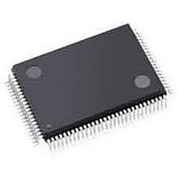
LFXP3C-3TN100I Lattice, LFXP3C-3TN100I Datasheet - Page 300

LFXP3C-3TN100I
Manufacturer Part Number
LFXP3C-3TN100I
Description
FPGA - Field Programmable Gate Array 3.1K LUTs 62 IO 1.8/ 2.5/3.3V -3 Spd I
Manufacturer
Lattice
Specifications of LFXP3C-3TN100I
Number Of Programmable I/os
62
Data Ram Size
55296
Supply Voltage (max)
3.465 V
Maximum Operating Temperature
+ 100 C
Minimum Operating Temperature
- 40 C
Mounting Style
SMD/SMT
Supply Voltage (min)
1.71 V
Package / Case
TQFP-100
Package
100TQFP
Family Name
LatticeXP
Device Logic Units
3000
Maximum Internal Frequency
320 MHz
Typical Operating Supply Voltage
1.8|2.5|3.3 V
Maximum Number Of User I/os
62
Ram Bits
55296
Re-programmability Support
Yes
Lead Free Status / RoHS Status
Lead free / RoHS Compliant
Available stocks
Company
Part Number
Manufacturer
Quantity
Price
Company:
Part Number:
LFXP3C-3TN100I
Manufacturer:
Lattice Semiconductor Corporation
Quantity:
10 000
- Current page: 300 of 397
- Download datasheet (10Mb)
LatticeXP sysCONFIG
Usage Guide
September 2008
Technical Note TN1082
Introduction
The memory in the LatticeXP™ FPGAs is built using Flash cells, along with SRAM cells, so that configuration
memory can be loaded automatically at power-up, or at any time the user wishes to update the device. In addition
to “instant-on” capability, on-chip Flash memory greatly increases design security by getting rid of the external con-
figuration bitstream; while maintaining the ease of use and reprogrammability of an SRAM-based FPGA.
While an external device is not required, the LatticeXP does support several external configuration modes. The
available external configuration modes are:
• Slave Serial
• Master Serial
• Slave Parallel
• ispJTAG™ (1149.1 interface)
This guide will cover all the configuration options available for the LatticeXP.
Programming Overview
The LatticeXP contains two types of memory, SRAM and Flash (refer to Figure 13-1). SRAM contains the FPGA
configuration, essentially the “fuses” that define the circuit connections; Flash provides an internal storage space
for the configuration data.
The SRAM can be configured using JTAG, one of the external configuration modes, or by using the data stored in
on-chip Flash. The configuration process consists of SRAM initialization (clear the RAM and the address pointers),
loading the SRAM with the configuration data, and setting the FPGA into user mode (waking up the FPGA).
On-chip Flash can be programmed by using JTAG or by using the external Slave Parallel port. JTAG Flash pro-
gramming can be performed any time the device is powered up. The Slave Parallel port uses the sysCONFIG™
pins and can program the Flash directly or in the background. Direct programming takes place during config mode,
background programming during user mode. The FPGA enters config mode at power up, when the PROGRAMN
pin is pulled low, or when a refresh command is issued via JTAG; it enters user mode when it wakes up, i.e. when
the device begins running user code. These two programming modes, direct and background, will be referred to in
this document as Flash Direct and Flash Background.
© 2008 Lattice Semiconductor Corp. All Lattice trademarks, registered trademarks, patents, and disclaimers are as listed at www.latticesemi.com/legal. All other brand
or product names are trademarks or registered trademarks of their respective holders. The specifications and information herein are subject to change without notice.
www.latticesemi.com
13-1
tn1082_01.9
Related parts for LFXP3C-3TN100I
Image
Part Number
Description
Manufacturer
Datasheet
Request
R

Part Number:
Description:
FPGA - Field Programmable Gate Array 3.1K LUTs 136 IO 1.8 /2.5/3.3V -3 Spd I
Manufacturer:
Lattice

Part Number:
Description:
FPGA - Field Programmable Gate Array 3.1K LUTs 62 IO 1.8/ 2.5/3.3V -3 Spd I
Manufacturer:
Lattice

Part Number:
Description:
FPGA - Field Programmable Gate Array 3.1K LUTs 136 IO 1.8 /2.5/3.3V -3 Spd
Manufacturer:
Lattice

Part Number:
Description:
FPGA - Field Programmable Gate Array 3.1K LUTs 100 I/O 1.8/2.5/3.3V -3 Spd
Manufacturer:
Lattice
Datasheet:

Part Number:
Description:
FPGA - Field Programmable Gate Array 3.1K LUTS 100 I/O
Manufacturer:
Lattice
Datasheet:

Part Number:
Description:
FPGA - Field Programmable Gate Array 3.1K LUTS 136 I/O
Manufacturer:
Lattice
Datasheet:

Part Number:
Description:
FPGA - Field Programmable Gate Array 3.1K LUTs 100 I/O 1.8/2.5/3.3V -4 Spd
Manufacturer:
Lattice
Datasheet:

Part Number:
Description:
FPGA - Field Programmable Gate Array 3.1K LUTS 62 I/O
Manufacturer:
Lattice
Datasheet:

Part Number:
Description:
FPGA - Field Programmable Gate Array 3.1K LUTs 62 I/O 1.8/2.5/3.3V -4 Spd
Manufacturer:
Lattice
Datasheet:

Part Number:
Description:
FPGA - Field Programmable Gate Array 3.1K LUTS 62 I/O
Manufacturer:
Lattice
Datasheet:

Part Number:
Description:
FPGA - Field Programmable Gate Array 3.1K LUTs 100 I/O 1.8/2.5/3.3V IND
Manufacturer:
Lattice
Datasheet:

Part Number:
Description:
FPGA, 1.8V FLASH, INSTANT ON, SMD
Manufacturer:
LATTICE SEMICONDUCTOR
Datasheet:
Part Number:
Description:
FPGA LatticeXP Family 3000 Cells 320MHz 130nm (CMOS) Technology 1.8V/2.5V/3.3V 208-Pin PQFP Tray
Manufacturer:
LATTICE SEMICONDUCTOR
Datasheet:
Part Number:
Description:
FPGA LatticeXP Family 3000 Cells 320MHz 130nm (CMOS) Technology 1.8V/2.5V/3.3V 144-Pin TQFP Tray
Manufacturer:
LATTICE SEMICONDUCTOR
Datasheet:
Part Number:
Description:
FPGA LatticeXP Family 3000 Cells 360MHz 130nm (CMOS) Technology 1.8V/2.5V/3.3V 100-Pin TQFP Tray
Manufacturer:
LATTICE SEMICONDUCTOR
Datasheet:


