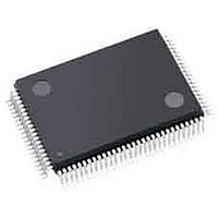
LFXP3C-3TN100I Lattice, LFXP3C-3TN100I Datasheet - Page 261

LFXP3C-3TN100I
Manufacturer Part Number
LFXP3C-3TN100I
Description
FPGA - Field Programmable Gate Array 3.1K LUTs 62 IO 1.8/ 2.5/3.3V -3 Spd I
Manufacturer
Lattice
Specifications of LFXP3C-3TN100I
Number Of Programmable I/os
62
Data Ram Size
55296
Supply Voltage (max)
3.465 V
Maximum Operating Temperature
+ 100 C
Minimum Operating Temperature
- 40 C
Mounting Style
SMD/SMT
Supply Voltage (min)
1.71 V
Package / Case
TQFP-100
Package
100TQFP
Family Name
LatticeXP
Device Logic Units
3000
Maximum Internal Frequency
320 MHz
Typical Operating Supply Voltage
1.8|2.5|3.3 V
Maximum Number Of User I/os
62
Ram Bits
55296
Re-programmability Support
Yes
Lead Free Status / RoHS Status
Lead free / RoHS Compliant
Available stocks
Company
Part Number
Manufacturer
Quantity
Price
Company:
Part Number:
LFXP3C-3TN100I
Manufacturer:
Lattice Semiconductor Corporation
Quantity:
10 000
- Current page: 261 of 397
- Download datasheet (10Mb)
Lattice Semiconductor
FDEL Settings
There are four ways the user can enter the desired FDEL value.
Table 11-2. LatticeECP/EC and LatticeXP PLL Attributes (Continued)
CLKOP Actual
Frequency
CLKOK Frequency
Tolerance
CLKOK Actual
Frequency
CLKI Divider
Setting
CLKFB Divider
Setting
CLKOP Divider
Setting
CLKOK Divider
Setting
Fine Delay Adjust
Coarse Phase Shift
Selection (O)
Duty Cycle Selection
(1/8 increment)
Delay Control
Feedback Mode
CLKOS Select
CLKOK Select
1. DYNAMIC: This mode switches delay control between Dynamic and Static depending upon the input logic of the DDAMODE pin.
2. The CLKOP_DIV value is calculated to maximize the f
3. The CLKOP Divider values are 2, 4, 6, 8,..32 (2, 4, 6, 8..30 for LatticeXP devices) if CLKOS is not used. The CLKOP Divider values are 2,
4. All divider settings are user transparent in Frequency Mode. These are user attributes in Divider Mode.
5. Refer to data sheet for frequency limits.
6. Values in parentheses are for LatticeXP devices.
7. This attribute is not available in the IPexpress GUI. After reviewing the trace report file, users can determine the amount of delay that will
STATIC: This is Static Control Only mode.
default value is 6. If CLKOS is used, the value is 4.
4, 8, 16, 32 (2, 4, 8, 16 for LatticeXP devices) if CLKOS is used.
best fit the clocking in their design. Further information on FDEL settings is described in the following section.
Accessible
1. Although the FDEL entry is not available in the IPexpress GUI, the module generated by IPexpress
2. Preference File: User may specify the preference in the Preference file.
3. Pre-Map Preference Editor: Users can enter the FDEL value in the Pre-Map Preference Editor as shown in
User
includes the attribute with default value, “0”. Users can replace it with a desired value.
Example of source code with default FDEL value:
Example:
Figure 11-4.
attribute FDEL of ehxpll_mod_0_0 : label is "0";
generic map (…
ASIC "FDEL_CODE_0_0" TYPE "EHXPLLB" FDEL="-2"
GUI Access
IPexpress
FDEL=>"0",
…
")
Y
Y
Y
Y
Y
Y
Y
N
Y
Y
Y
Y
Y
Y
CLKI_DIV
CLKFB_DIV
CLKOP_DIV
CLKOK_DIV
FDEL
PHASEADJ
DUTY
DELAY_CNTL1
FB_MODE
Attribute
4, 6
Name
6
6
VCO
Preference
Language
Support
within the specified range. For LatticeXP devices, if CLKOS is not used, the
N
N
N
Y
Y
Y
Y
Y
Y
Y
Y
N
N
N
11-5
Preference
Support
Editor
N
N
N
N
N
N
N
Y
N
N
N
N
N
N
sysCLOCK PLL Design and Usage Guide
INTERNAL/CLOCKTREE/EXTERNAL
0.0, 0.1, 0.2, 0.5,1.0, 2.0, 5.0, 10.0
DYNAMIC/STATIC
2, 4, 6,..,126, 128
1 to 16 (1 to 15)
1 to 16 (1 to 15)
0, 45, 90...315
LatticeECP/EC and LatticeXP
Note 3
-8 to 8
Value
1 to 7
;
CLOCKTREE
8
Default
2
STATIC
Value
(4 or 6)
0.0
1
1
2
0
0
4
Degrees
Units
MHz
MHz
ps
%
Related parts for LFXP3C-3TN100I
Image
Part Number
Description
Manufacturer
Datasheet
Request
R

Part Number:
Description:
FPGA - Field Programmable Gate Array 3.1K LUTs 136 IO 1.8 /2.5/3.3V -3 Spd I
Manufacturer:
Lattice

Part Number:
Description:
FPGA - Field Programmable Gate Array 3.1K LUTs 62 IO 1.8/ 2.5/3.3V -3 Spd I
Manufacturer:
Lattice

Part Number:
Description:
FPGA - Field Programmable Gate Array 3.1K LUTs 136 IO 1.8 /2.5/3.3V -3 Spd
Manufacturer:
Lattice

Part Number:
Description:
FPGA - Field Programmable Gate Array 3.1K LUTs 100 I/O 1.8/2.5/3.3V -3 Spd
Manufacturer:
Lattice
Datasheet:

Part Number:
Description:
FPGA - Field Programmable Gate Array 3.1K LUTS 100 I/O
Manufacturer:
Lattice
Datasheet:

Part Number:
Description:
FPGA - Field Programmable Gate Array 3.1K LUTS 136 I/O
Manufacturer:
Lattice
Datasheet:

Part Number:
Description:
FPGA - Field Programmable Gate Array 3.1K LUTs 100 I/O 1.8/2.5/3.3V -4 Spd
Manufacturer:
Lattice
Datasheet:

Part Number:
Description:
FPGA - Field Programmable Gate Array 3.1K LUTS 62 I/O
Manufacturer:
Lattice
Datasheet:

Part Number:
Description:
FPGA - Field Programmable Gate Array 3.1K LUTs 62 I/O 1.8/2.5/3.3V -4 Spd
Manufacturer:
Lattice
Datasheet:

Part Number:
Description:
FPGA - Field Programmable Gate Array 3.1K LUTS 62 I/O
Manufacturer:
Lattice
Datasheet:

Part Number:
Description:
FPGA - Field Programmable Gate Array 3.1K LUTs 100 I/O 1.8/2.5/3.3V IND
Manufacturer:
Lattice
Datasheet:

Part Number:
Description:
FPGA, 1.8V FLASH, INSTANT ON, SMD
Manufacturer:
LATTICE SEMICONDUCTOR
Datasheet:
Part Number:
Description:
FPGA LatticeXP Family 3000 Cells 320MHz 130nm (CMOS) Technology 1.8V/2.5V/3.3V 208-Pin PQFP Tray
Manufacturer:
LATTICE SEMICONDUCTOR
Datasheet:
Part Number:
Description:
FPGA LatticeXP Family 3000 Cells 320MHz 130nm (CMOS) Technology 1.8V/2.5V/3.3V 144-Pin TQFP Tray
Manufacturer:
LATTICE SEMICONDUCTOR
Datasheet:
Part Number:
Description:
FPGA LatticeXP Family 3000 Cells 360MHz 130nm (CMOS) Technology 1.8V/2.5V/3.3V 100-Pin TQFP Tray
Manufacturer:
LATTICE SEMICONDUCTOR
Datasheet:


