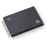
LFXP3C-3TN100I Lattice, LFXP3C-3TN100I Datasheet - Page 356

LFXP3C-3TN100I
Manufacturer Part Number
LFXP3C-3TN100I
Description
FPGA - Field Programmable Gate Array 3.1K LUTs 62 IO 1.8/ 2.5/3.3V -3 Spd I
Manufacturer
Lattice
Specifications of LFXP3C-3TN100I
Number Of Programmable I/os
62
Data Ram Size
55296
Supply Voltage (max)
3.465 V
Maximum Operating Temperature
+ 100 C
Minimum Operating Temperature
- 40 C
Mounting Style
SMD/SMT
Supply Voltage (min)
1.71 V
Package / Case
TQFP-100
Package
100TQFP
Family Name
LatticeXP
Device Logic Units
3000
Maximum Internal Frequency
320 MHz
Typical Operating Supply Voltage
1.8|2.5|3.3 V
Maximum Number Of User I/os
62
Ram Bits
55296
Re-programmability Support
Yes
Lead Free Status / RoHS Status
Lead free / RoHS Compliant
Available stocks
Company
Part Number
Manufacturer
Quantity
Price
Company:
Part Number:
LFXP3C-3TN100I
Manufacturer:
Lattice Semiconductor Corporation
Quantity:
10 000
- Current page: 356 of 397
- Download datasheet (10Mb)
Lattice Semiconductor
example, the NCD file with the best timing score would be saved. The tool keeps track of the timing and routing per-
formance for every iteration in a file called the multiple par report (.par). Such a file is shown in Figure 17-10.
Figure 17-10. Multiple PAR Report (.par)
Figure 17-10 indicates that:
Note that, in Figure 17-8, if “Placement Iterations (0=run until solved)” is set to 0, the tool will run indefinitely
through multiple iterations until a 0 timing score is reached. In a design that is known to have large timing violations,
a 0 timing score will never be reached. As a consequence, the user must intervene and stop the flow at a given
point in time.
In general, multiple placement iterations can help placement but can also use many CPU cycles. Multiple place-
ment iterations should be used carefully due to system limitations and the uncertainty of results. It is better to fix the
root cause of timing problems in the design stage.
Clock Boosting
Clock boosting, supported in Lattice Semiconductor’s ORCA Series device family, is the deliberate introduction of
clock skew on a target flop to increase the setup margin. Every programmable flip-flop in the device has program-
mable delay elements before clock inputs for this purpose. The automated clock boosting tool will attempt to meet
setup constraints by introducing delays to as many target registers as needed to meet timing, in effect, borrow reg-
ister hold margins to meet register set-up timing. The following bullets summarize how clock boosting is accom-
plished in Lattice Semiconductor ORCA Series device family.
• The “5_” under the Level/Cost column means that the Placement Effort level was set to 5. The Placement
• 10 different iterations ran (10 cost tables).
• Timing scores are expressed in total picoseconds (ps) by which the design is missing constraints on all
• Iteration number 4 (cost table 4) achieved a 0 timing score and hence was the design saved. More than one
• Each iteration routed completely.
• A 4-tap delay cell structure in front of the clock port of every flip-flop in the device (includes I/O flip-flops)
• Ability to borrow clock cycle time from one easily-met path and give this time to a difficult-to-meet path
Effort level can range from 1 (lowest) to 5 (highest).
preferences.
.ncd file can be saved. This is user-controlled via the “Placement Save Best Runs” value box shown in
Figure 17-8.
Level/
Cost [ncd]
----------
5_4
5_6
5_2
5_7
5_3
5_10
5_1
5_8
5_5
5_9
* : Design saved.
*
Number
Unrouted
--------
0
0
0
0
0
0
0
0
0
0
Timing
Score
-------
0
25
102
158
186
318
470
562
732
844
17-12
Run
Time
-----
01:58
02:01
01:45
02:15
01:54
02:39
01:51
02:25
02:00
02:27
Lattice Semiconductor FPGA
Successful Place and Route
NCD
Status
--------
Complete
Complete
Complete
Complete
Complete
Complete
Complete
Complete
Complete
Complete
Related parts for LFXP3C-3TN100I
Image
Part Number
Description
Manufacturer
Datasheet
Request
R

Part Number:
Description:
FPGA - Field Programmable Gate Array 3.1K LUTs 136 IO 1.8 /2.5/3.3V -3 Spd I
Manufacturer:
Lattice

Part Number:
Description:
FPGA - Field Programmable Gate Array 3.1K LUTs 62 IO 1.8/ 2.5/3.3V -3 Spd I
Manufacturer:
Lattice

Part Number:
Description:
FPGA - Field Programmable Gate Array 3.1K LUTs 136 IO 1.8 /2.5/3.3V -3 Spd
Manufacturer:
Lattice

Part Number:
Description:
FPGA - Field Programmable Gate Array 3.1K LUTs 100 I/O 1.8/2.5/3.3V -3 Spd
Manufacturer:
Lattice
Datasheet:

Part Number:
Description:
FPGA - Field Programmable Gate Array 3.1K LUTS 100 I/O
Manufacturer:
Lattice
Datasheet:

Part Number:
Description:
FPGA - Field Programmable Gate Array 3.1K LUTS 136 I/O
Manufacturer:
Lattice
Datasheet:

Part Number:
Description:
FPGA - Field Programmable Gate Array 3.1K LUTs 100 I/O 1.8/2.5/3.3V -4 Spd
Manufacturer:
Lattice
Datasheet:

Part Number:
Description:
FPGA - Field Programmable Gate Array 3.1K LUTS 62 I/O
Manufacturer:
Lattice
Datasheet:

Part Number:
Description:
FPGA - Field Programmable Gate Array 3.1K LUTs 62 I/O 1.8/2.5/3.3V -4 Spd
Manufacturer:
Lattice
Datasheet:

Part Number:
Description:
FPGA - Field Programmable Gate Array 3.1K LUTS 62 I/O
Manufacturer:
Lattice
Datasheet:

Part Number:
Description:
FPGA - Field Programmable Gate Array 3.1K LUTs 100 I/O 1.8/2.5/3.3V IND
Manufacturer:
Lattice
Datasheet:

Part Number:
Description:
FPGA, 1.8V FLASH, INSTANT ON, SMD
Manufacturer:
LATTICE SEMICONDUCTOR
Datasheet:
Part Number:
Description:
FPGA LatticeXP Family 3000 Cells 320MHz 130nm (CMOS) Technology 1.8V/2.5V/3.3V 208-Pin PQFP Tray
Manufacturer:
LATTICE SEMICONDUCTOR
Datasheet:
Part Number:
Description:
FPGA LatticeXP Family 3000 Cells 320MHz 130nm (CMOS) Technology 1.8V/2.5V/3.3V 144-Pin TQFP Tray
Manufacturer:
LATTICE SEMICONDUCTOR
Datasheet:
Part Number:
Description:
FPGA LatticeXP Family 3000 Cells 360MHz 130nm (CMOS) Technology 1.8V/2.5V/3.3V 100-Pin TQFP Tray
Manufacturer:
LATTICE SEMICONDUCTOR
Datasheet:


