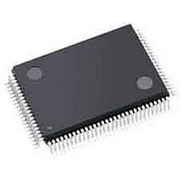
LFXP3C-3TN100I Lattice, LFXP3C-3TN100I Datasheet - Page 188

LFXP3C-3TN100I
Manufacturer Part Number
LFXP3C-3TN100I
Description
FPGA - Field Programmable Gate Array 3.1K LUTs 62 IO 1.8/ 2.5/3.3V -3 Spd I
Manufacturer
Lattice
Specifications of LFXP3C-3TN100I
Number Of Programmable I/os
62
Data Ram Size
55296
Supply Voltage (max)
3.465 V
Maximum Operating Temperature
+ 100 C
Minimum Operating Temperature
- 40 C
Mounting Style
SMD/SMT
Supply Voltage (min)
1.71 V
Package / Case
TQFP-100
Package
100TQFP
Family Name
LatticeXP
Device Logic Units
3000
Maximum Internal Frequency
320 MHz
Typical Operating Supply Voltage
1.8|2.5|3.3 V
Maximum Number Of User I/os
62
Ram Bits
55296
Re-programmability Support
Yes
Lead Free Status / RoHS Status
Lead free / RoHS Compliant
Available stocks
Company
Part Number
Manufacturer
Quantity
Price
Company:
Part Number:
LFXP3C-3TN100I
Manufacturer:
Lattice Semiconductor Corporation
Quantity:
10 000
- Current page: 188 of 397
- Download datasheet (10Mb)
Lattice Semiconductor
Table 9-7. EBR based Pseudo-Dual Port Memory Port Definitions
Reset (or RST) only resets the input and output registers of the RAM. It does not reset the contents of the memory.
CS, or Chip Select, a port available in the EBR primitive, is useful when memory requires multiple EBR blocks to be
cascaded. The CS signal forms the MSB for the address when multiple EBR blocks are cascaded. CS is a 3-bit
bus, so it can cascade eight memories easily. However, if the memory size specified by the user requires more than
eight EBR blocks, the software automatically generates the additional address decoding logic, which is imple-
mented in the PFU (external to the EBR blocks).
Each EBR block consists of 9,216 bits of RAM. The values for x (for Address) and y (Data) for each EBR block for
the devices are included in Table 9-8.
Table 9-8. Pseudo-Dual Port Memory Sizes for 9K Memory for LatticeECP/EC and LatticeXP Devices
Table 9-9 shows the various attributes available for the Pseudo Dual Port Memory (RAM_DP). Some of these attri-
butes are user selectable through the IPexpress GUI. For detailed attribute definitions, refer to Appendix A.
Pseudo-Dual
Port Memory
512 x 18
8K x 1
4K x 2
2K x 4
1K x 9
Size
RdAddress
WrAddress
RdClock
WrClock
RdClockEn
WrClockEn
Q
Data
WE
Reset
—
Generated Module
Port Name in
Input Data
DIA[17:0]
DIA[1:0]
DIA[3:0]
DIA[8:0]
Port A
DIA
ADR[x:0]
ADW[x:0]
CLKR
CLKW
CER
CEW
DO[y:0]
DI[y:0]
WE
RST
CS[2:0]
Port Name in the EBR
Input Data
DIB[17:0]
DIB[1:0]
DIB[3:0]
DIB[8:0]
Block Primitive
Port B
DIB
Output Data
DOA[17:0]
DOA[1:0]
DOA[3:0]
DOA[8:0]
Port A
DOA
9-23
Read Address
Write Address
Read Clock
Write Clock
Read Clock Enable
Write Clock Enable
Read Data
Write Data
Write Enable
Reset
Chip Select
Description
LatticeECP/EC and LatticeXP Devices
Output Data
DOB[17:0]
DOB[1:0]
DOB[3:0]
DOB[8:0]
Port B
DOB
—
—
Rising Clock Edge
Rising Clock Edge
Active High
Active High
—
—
Active High
Active High
—
Read Address
[MSB:LSB]
RAD[12:0]
RAD[11:0]
RAD[10:0]
RAD[9:0]
RAD[9:0]
Memory Usage Guide
Port A
Active State
Write Address
[MSB:LSB]
WAD[12:0]
WAD[11:0]
WAD[10:0]
WAD[9:0]
WAD[9:0]
Port B
Related parts for LFXP3C-3TN100I
Image
Part Number
Description
Manufacturer
Datasheet
Request
R

Part Number:
Description:
FPGA - Field Programmable Gate Array 3.1K LUTs 136 IO 1.8 /2.5/3.3V -3 Spd I
Manufacturer:
Lattice

Part Number:
Description:
FPGA - Field Programmable Gate Array 3.1K LUTs 62 IO 1.8/ 2.5/3.3V -3 Spd I
Manufacturer:
Lattice

Part Number:
Description:
FPGA - Field Programmable Gate Array 3.1K LUTs 136 IO 1.8 /2.5/3.3V -3 Spd
Manufacturer:
Lattice

Part Number:
Description:
FPGA - Field Programmable Gate Array 3.1K LUTs 100 I/O 1.8/2.5/3.3V -3 Spd
Manufacturer:
Lattice
Datasheet:

Part Number:
Description:
FPGA - Field Programmable Gate Array 3.1K LUTS 100 I/O
Manufacturer:
Lattice
Datasheet:

Part Number:
Description:
FPGA - Field Programmable Gate Array 3.1K LUTS 136 I/O
Manufacturer:
Lattice
Datasheet:

Part Number:
Description:
FPGA - Field Programmable Gate Array 3.1K LUTs 100 I/O 1.8/2.5/3.3V -4 Spd
Manufacturer:
Lattice
Datasheet:

Part Number:
Description:
FPGA - Field Programmable Gate Array 3.1K LUTS 62 I/O
Manufacturer:
Lattice
Datasheet:

Part Number:
Description:
FPGA - Field Programmable Gate Array 3.1K LUTs 62 I/O 1.8/2.5/3.3V -4 Spd
Manufacturer:
Lattice
Datasheet:

Part Number:
Description:
FPGA - Field Programmable Gate Array 3.1K LUTS 62 I/O
Manufacturer:
Lattice
Datasheet:

Part Number:
Description:
FPGA - Field Programmable Gate Array 3.1K LUTs 100 I/O 1.8/2.5/3.3V IND
Manufacturer:
Lattice
Datasheet:

Part Number:
Description:
FPGA, 1.8V FLASH, INSTANT ON, SMD
Manufacturer:
LATTICE SEMICONDUCTOR
Datasheet:
Part Number:
Description:
FPGA LatticeXP Family 3000 Cells 320MHz 130nm (CMOS) Technology 1.8V/2.5V/3.3V 208-Pin PQFP Tray
Manufacturer:
LATTICE SEMICONDUCTOR
Datasheet:
Part Number:
Description:
FPGA LatticeXP Family 3000 Cells 320MHz 130nm (CMOS) Technology 1.8V/2.5V/3.3V 144-Pin TQFP Tray
Manufacturer:
LATTICE SEMICONDUCTOR
Datasheet:
Part Number:
Description:
FPGA LatticeXP Family 3000 Cells 360MHz 130nm (CMOS) Technology 1.8V/2.5V/3.3V 100-Pin TQFP Tray
Manufacturer:
LATTICE SEMICONDUCTOR
Datasheet:


