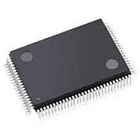
LFXP3C-3TN100I Lattice, LFXP3C-3TN100I Datasheet - Page 248

LFXP3C-3TN100I
Manufacturer Part Number
LFXP3C-3TN100I
Description
FPGA - Field Programmable Gate Array 3.1K LUTs 62 IO 1.8/ 2.5/3.3V -3 Spd I
Manufacturer
Lattice
Specifications of LFXP3C-3TN100I
Number Of Programmable I/os
62
Data Ram Size
55296
Supply Voltage (max)
3.465 V
Maximum Operating Temperature
+ 100 C
Minimum Operating Temperature
- 40 C
Mounting Style
SMD/SMT
Supply Voltage (min)
1.71 V
Package / Case
TQFP-100
Package
100TQFP
Family Name
LatticeXP
Device Logic Units
3000
Maximum Internal Frequency
320 MHz
Typical Operating Supply Voltage
1.8|2.5|3.3 V
Maximum Number Of User I/os
62
Ram Bits
55296
Re-programmability Support
Yes
Lead Free Status / RoHS Status
Lead free / RoHS Compliant
Available stocks
Company
Part Number
Manufacturer
Quantity
Price
Company:
Part Number:
LFXP3C-3TN100I
Manufacturer:
Lattice Semiconductor Corporation
Quantity:
10 000
- Current page: 248 of 397
- Download datasheet (10Mb)
Lattice Semiconductor
Appendix D. Generic (Non-Memory) High-Speed DDR Interface
The following HDL implements the DDR input interface using PFU registers for non-memory DDR applications.
VHDL Implementation
library IEEE;
use IEEE.std_logic_1164.all;
library ec;
use ec.components.all;
entity ddrin is
end ddrin;
architecture structure of ddrin is
-- parameterized module component declaration
component pll90
end component;
attribute syn_useioff : boolean;
attribute syn_useioff of structure : architecture is false;
begin
demux: process (rst, ddrclk90)
begin
port (rst : in std_logic;
port (CLK: in std_logic; RESET: in std_logic; CLKOP: out std_logic;
ddrclk: in std_logic;
ddrdata: in std_logic_vector(7 downto 0);
datap: out std_logic_vector(7 downto 0);
datan: out std_logic_vector(7 downto 0));
-- parameterized module component instance
signal pos0 : std_logic_vector( 7 downto 0 );
signal pos1 : std_logic_vector( 7 downto 0 );
signal neg0 : std_logic_vector( 7 downto 0 );
signal clklock : std_logic;
signal ddrclk0: std_logic;
signal ddrclk90: std_logic;
signal vcc_net : std_logic;
signal gnd_net: std_logic;
vcc_net <= '1';
gnd_net <= '0';
I0 : pll90
port map (CLK=>ddrclk, RESET=>rst, CLKOP=>ddrclk0, CLKOS=>ddrclk90, LOCK=>clklock);
if
elsif rising_edge(ddrclk90) then
CLKOS: out std_logic; LOCK: out std_logic);
rst = '1' then
pos0
neg0
pos1
pos0
<= (others => '0');
<= (others => '0');
<= (others => '0');
<= ddrdata;
10-29
LatticeECP/EC and LatticeXP
DDR Usage Guide
Related parts for LFXP3C-3TN100I
Image
Part Number
Description
Manufacturer
Datasheet
Request
R

Part Number:
Description:
FPGA - Field Programmable Gate Array 3.1K LUTs 136 IO 1.8 /2.5/3.3V -3 Spd I
Manufacturer:
Lattice

Part Number:
Description:
FPGA - Field Programmable Gate Array 3.1K LUTs 62 IO 1.8/ 2.5/3.3V -3 Spd I
Manufacturer:
Lattice

Part Number:
Description:
FPGA - Field Programmable Gate Array 3.1K LUTs 136 IO 1.8 /2.5/3.3V -3 Spd
Manufacturer:
Lattice

Part Number:
Description:
FPGA - Field Programmable Gate Array 3.1K LUTs 100 I/O 1.8/2.5/3.3V -3 Spd
Manufacturer:
Lattice
Datasheet:

Part Number:
Description:
FPGA - Field Programmable Gate Array 3.1K LUTS 100 I/O
Manufacturer:
Lattice
Datasheet:

Part Number:
Description:
FPGA - Field Programmable Gate Array 3.1K LUTS 136 I/O
Manufacturer:
Lattice
Datasheet:

Part Number:
Description:
FPGA - Field Programmable Gate Array 3.1K LUTs 100 I/O 1.8/2.5/3.3V -4 Spd
Manufacturer:
Lattice
Datasheet:

Part Number:
Description:
FPGA - Field Programmable Gate Array 3.1K LUTS 62 I/O
Manufacturer:
Lattice
Datasheet:

Part Number:
Description:
FPGA - Field Programmable Gate Array 3.1K LUTs 62 I/O 1.8/2.5/3.3V -4 Spd
Manufacturer:
Lattice
Datasheet:

Part Number:
Description:
FPGA - Field Programmable Gate Array 3.1K LUTS 62 I/O
Manufacturer:
Lattice
Datasheet:

Part Number:
Description:
FPGA - Field Programmable Gate Array 3.1K LUTs 100 I/O 1.8/2.5/3.3V IND
Manufacturer:
Lattice
Datasheet:

Part Number:
Description:
FPGA, 1.8V FLASH, INSTANT ON, SMD
Manufacturer:
LATTICE SEMICONDUCTOR
Datasheet:
Part Number:
Description:
FPGA LatticeXP Family 3000 Cells 320MHz 130nm (CMOS) Technology 1.8V/2.5V/3.3V 208-Pin PQFP Tray
Manufacturer:
LATTICE SEMICONDUCTOR
Datasheet:
Part Number:
Description:
FPGA LatticeXP Family 3000 Cells 320MHz 130nm (CMOS) Technology 1.8V/2.5V/3.3V 144-Pin TQFP Tray
Manufacturer:
LATTICE SEMICONDUCTOR
Datasheet:
Part Number:
Description:
FPGA LatticeXP Family 3000 Cells 360MHz 130nm (CMOS) Technology 1.8V/2.5V/3.3V 100-Pin TQFP Tray
Manufacturer:
LATTICE SEMICONDUCTOR
Datasheet:


