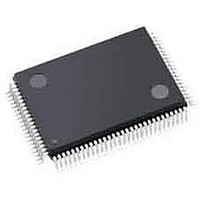
LFXP3C-3TN100I Lattice, LFXP3C-3TN100I Datasheet - Page 276

LFXP3C-3TN100I
Manufacturer Part Number
LFXP3C-3TN100I
Description
FPGA - Field Programmable Gate Array 3.1K LUTs 62 IO 1.8/ 2.5/3.3V -3 Spd I
Manufacturer
Lattice
Specifications of LFXP3C-3TN100I
Number Of Programmable I/os
62
Data Ram Size
55296
Supply Voltage (max)
3.465 V
Maximum Operating Temperature
+ 100 C
Minimum Operating Temperature
- 40 C
Mounting Style
SMD/SMT
Supply Voltage (min)
1.71 V
Package / Case
TQFP-100
Package
100TQFP
Family Name
LatticeXP
Device Logic Units
3000
Maximum Internal Frequency
320 MHz
Typical Operating Supply Voltage
1.8|2.5|3.3 V
Maximum Number Of User I/os
62
Ram Bits
55296
Re-programmability Support
Yes
Lead Free Status / RoHS Status
Lead free / RoHS Compliant
Available stocks
Company
Part Number
Manufacturer
Quantity
Price
Company:
Part Number:
LFXP3C-3TN100I
Manufacturer:
Lattice Semiconductor Corporation
Quantity:
10 000
- Current page: 276 of 397
- Download datasheet (10Mb)
Lattice Semiconductor
Appendix A. Clock Preferences
A few key clock preferences are introduced below. Refer to the ‘Help’ file for other preferences and detailed infor-
mation.
ASIC
The following preference command assigns a phase of 90° to the CIMDLLA CLKOP.
FREQUENCY
The following physical preference command assigns a frequency of 100 MHz to a net named clk1.
The following preference specifies a hold margin value for each clock domain.
MAXSKEW
The following command assigns a maximum skew of 5 ns to a net named NetB.
MULTICYCLE
The following command will relax the period to 50 ns for the path starting at COMPA to COMPB (NET1).
PERIOD
The following command assigns a clock period of 30 ns to the port named Clk1.
PROHIBIT
This command prohibits the use of a primary clock to route a clock net named bf_clk.
CLOCK_TO_OUT
Specifies a maximum allowable output delay relative to a clock.
Below are two preferences using both the CLKPORT and CLKNET keywords showing the corresponding scope of
TRACE reporting.
The CLKNET will stop tracing the path before the PLL, so you will not get PLL compensation timing numbers.
The above preference will yield the following clock path:
ASIC "my_pll" TYPE "EXHXPLLB" CLKOS_PHASE=90;
FREQUENCY NET "clk1" 100 MHz;
FREQUENCY NET "RX_CLKA_CMOS_c" 100.000 MHz HOLD_MARGIN 1 ns;
MAXSKEW NET "NetB" 5 NS;
MULTICYCLE "PATH1" START COMP "COMPA" END COMP "COMPB" NET "NET1" 50 NS ;
PERIOD PORT "Clk1" 30 NS;
PROHIBIT PRIMARY NET "bf_clk";
CLOCK_TO_OUT PORT "RxAddr_0" 6.000000 ns CLKNET "pll_rxclk" ;
11-20
sysCLOCK PLL Design and Usage Guide
LatticeECP/EC and LatticeXP
Related parts for LFXP3C-3TN100I
Image
Part Number
Description
Manufacturer
Datasheet
Request
R

Part Number:
Description:
FPGA - Field Programmable Gate Array 3.1K LUTs 136 IO 1.8 /2.5/3.3V -3 Spd I
Manufacturer:
Lattice

Part Number:
Description:
FPGA - Field Programmable Gate Array 3.1K LUTs 62 IO 1.8/ 2.5/3.3V -3 Spd I
Manufacturer:
Lattice

Part Number:
Description:
FPGA - Field Programmable Gate Array 3.1K LUTs 136 IO 1.8 /2.5/3.3V -3 Spd
Manufacturer:
Lattice

Part Number:
Description:
FPGA - Field Programmable Gate Array 3.1K LUTs 100 I/O 1.8/2.5/3.3V -3 Spd
Manufacturer:
Lattice
Datasheet:

Part Number:
Description:
FPGA - Field Programmable Gate Array 3.1K LUTS 100 I/O
Manufacturer:
Lattice
Datasheet:

Part Number:
Description:
FPGA - Field Programmable Gate Array 3.1K LUTS 136 I/O
Manufacturer:
Lattice
Datasheet:

Part Number:
Description:
FPGA - Field Programmable Gate Array 3.1K LUTs 100 I/O 1.8/2.5/3.3V -4 Spd
Manufacturer:
Lattice
Datasheet:

Part Number:
Description:
FPGA - Field Programmable Gate Array 3.1K LUTS 62 I/O
Manufacturer:
Lattice
Datasheet:

Part Number:
Description:
FPGA - Field Programmable Gate Array 3.1K LUTs 62 I/O 1.8/2.5/3.3V -4 Spd
Manufacturer:
Lattice
Datasheet:

Part Number:
Description:
FPGA - Field Programmable Gate Array 3.1K LUTS 62 I/O
Manufacturer:
Lattice
Datasheet:

Part Number:
Description:
FPGA - Field Programmable Gate Array 3.1K LUTs 100 I/O 1.8/2.5/3.3V IND
Manufacturer:
Lattice
Datasheet:

Part Number:
Description:
FPGA, 1.8V FLASH, INSTANT ON, SMD
Manufacturer:
LATTICE SEMICONDUCTOR
Datasheet:
Part Number:
Description:
FPGA LatticeXP Family 3000 Cells 320MHz 130nm (CMOS) Technology 1.8V/2.5V/3.3V 208-Pin PQFP Tray
Manufacturer:
LATTICE SEMICONDUCTOR
Datasheet:
Part Number:
Description:
FPGA LatticeXP Family 3000 Cells 320MHz 130nm (CMOS) Technology 1.8V/2.5V/3.3V 144-Pin TQFP Tray
Manufacturer:
LATTICE SEMICONDUCTOR
Datasheet:
Part Number:
Description:
FPGA LatticeXP Family 3000 Cells 360MHz 130nm (CMOS) Technology 1.8V/2.5V/3.3V 100-Pin TQFP Tray
Manufacturer:
LATTICE SEMICONDUCTOR
Datasheet:


