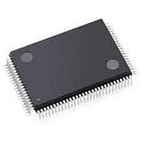
LFXP3C-3TN100I Lattice, LFXP3C-3TN100I Datasheet - Page 234

LFXP3C-3TN100I
Manufacturer Part Number
LFXP3C-3TN100I
Description
FPGA - Field Programmable Gate Array 3.1K LUTs 62 IO 1.8/ 2.5/3.3V -3 Spd I
Manufacturer
Lattice
Specifications of LFXP3C-3TN100I
Number Of Programmable I/os
62
Data Ram Size
55296
Supply Voltage (max)
3.465 V
Maximum Operating Temperature
+ 100 C
Minimum Operating Temperature
- 40 C
Mounting Style
SMD/SMT
Supply Voltage (min)
1.71 V
Package / Case
TQFP-100
Package
100TQFP
Family Name
LatticeXP
Device Logic Units
3000
Maximum Internal Frequency
320 MHz
Typical Operating Supply Voltage
1.8|2.5|3.3 V
Maximum Number Of User I/os
62
Ram Bits
55296
Re-programmability Support
Yes
Lead Free Status / RoHS Status
Lead free / RoHS Compliant
Available stocks
Company
Part Number
Manufacturer
Quantity
Price
Company:
Part Number:
LFXP3C-3TN100I
Manufacturer:
Lattice Semiconductor Corporation
Quantity:
10 000
- Current page: 234 of 397
- Download datasheet (10Mb)
Lattice Semiconductor
Internally the DQS and ADDR/CMD signals are clocked using the primary FPGA clock. Therefore, the user will
need to do a 1/4 (one-quarter) clock transfer from the core logic to the DDR registers. Timing can be hard to meet,
so it is recommended that the user first register these signals with the inverted Clock, so that the transfer from the
core logic to I/O registers will only require a 1/2 (half) clock transfer.
The data DQ and DM needs to be delayed by 90° as it leaves the FPGA. This is to center the data and data mask
relative to the DQS when it reaches the DDR memory. This can be accomplished by inverting the CLK to the DQ
and DM data.
The DM signal is generated using the same clock as the DQ data pin. The memory masks the DQ signals if the DM
pins are driven high.
The tristate control for the data output can also be implemented using the ODDRXB primitive.
Figure 10-16 illustrates how to hook up the ODDRXB primitives and the PLL. The DDR Software Primitives section
describes each of the primitives and its instantiation in more detail. Appendix A and Appendix B provide example
code for implementing the complete I/O section of a memory interface for a LatticeECP/EC or LatticeXP device.
Figure 10-16. Software Primitive Implementation for Memory Write
CLK
User logic)
(From
PLL
CLK + 90
CLK
D
D
D
D
D
User logic)
Q
Q
Q
Q
Q
(From
Core Logic
dataout_p
dataout_n
datatri_p
datatri_n
dqstri_p
dqstri_n
“0”
“1”
“0”
“1”
PIO Logic
10-15
CLK
DB
LSR
D
CLK
CLK
CLK
CLK
DA
LSR
LSR
LSR
LSR
CLK
DA
DB
DA
DB
DA
DB
DA
DB
LSR
DA
DB
ODDRXB
ODDRXB
ODDRXB
ODDRXB
ODDRXB
ODDRXB
Q
Q
Q
Q
Q
Q
Q
Q
LatticeECP/EC and LatticeXP
ADDR/
CLKP
CLKN
CMD
DQS
DQ
DM
DDR Usage Guide
DDR Memory
Device
Related parts for LFXP3C-3TN100I
Image
Part Number
Description
Manufacturer
Datasheet
Request
R

Part Number:
Description:
FPGA - Field Programmable Gate Array 3.1K LUTs 136 IO 1.8 /2.5/3.3V -3 Spd I
Manufacturer:
Lattice

Part Number:
Description:
FPGA - Field Programmable Gate Array 3.1K LUTs 62 IO 1.8/ 2.5/3.3V -3 Spd I
Manufacturer:
Lattice

Part Number:
Description:
FPGA - Field Programmable Gate Array 3.1K LUTs 136 IO 1.8 /2.5/3.3V -3 Spd
Manufacturer:
Lattice

Part Number:
Description:
FPGA - Field Programmable Gate Array 3.1K LUTs 100 I/O 1.8/2.5/3.3V -3 Spd
Manufacturer:
Lattice
Datasheet:

Part Number:
Description:
FPGA - Field Programmable Gate Array 3.1K LUTS 100 I/O
Manufacturer:
Lattice
Datasheet:

Part Number:
Description:
FPGA - Field Programmable Gate Array 3.1K LUTS 136 I/O
Manufacturer:
Lattice
Datasheet:

Part Number:
Description:
FPGA - Field Programmable Gate Array 3.1K LUTs 100 I/O 1.8/2.5/3.3V -4 Spd
Manufacturer:
Lattice
Datasheet:

Part Number:
Description:
FPGA - Field Programmable Gate Array 3.1K LUTS 62 I/O
Manufacturer:
Lattice
Datasheet:

Part Number:
Description:
FPGA - Field Programmable Gate Array 3.1K LUTs 62 I/O 1.8/2.5/3.3V -4 Spd
Manufacturer:
Lattice
Datasheet:

Part Number:
Description:
FPGA - Field Programmable Gate Array 3.1K LUTS 62 I/O
Manufacturer:
Lattice
Datasheet:

Part Number:
Description:
FPGA - Field Programmable Gate Array 3.1K LUTs 100 I/O 1.8/2.5/3.3V IND
Manufacturer:
Lattice
Datasheet:

Part Number:
Description:
FPGA, 1.8V FLASH, INSTANT ON, SMD
Manufacturer:
LATTICE SEMICONDUCTOR
Datasheet:
Part Number:
Description:
FPGA LatticeXP Family 3000 Cells 320MHz 130nm (CMOS) Technology 1.8V/2.5V/3.3V 208-Pin PQFP Tray
Manufacturer:
LATTICE SEMICONDUCTOR
Datasheet:
Part Number:
Description:
FPGA LatticeXP Family 3000 Cells 320MHz 130nm (CMOS) Technology 1.8V/2.5V/3.3V 144-Pin TQFP Tray
Manufacturer:
LATTICE SEMICONDUCTOR
Datasheet:
Part Number:
Description:
FPGA LatticeXP Family 3000 Cells 360MHz 130nm (CMOS) Technology 1.8V/2.5V/3.3V 100-Pin TQFP Tray
Manufacturer:
LATTICE SEMICONDUCTOR
Datasheet:


