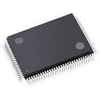
LFXP3C-3TN100I Lattice, LFXP3C-3TN100I Datasheet - Page 142

LFXP3C-3TN100I
Manufacturer Part Number
LFXP3C-3TN100I
Description
FPGA - Field Programmable Gate Array 3.1K LUTs 62 IO 1.8/ 2.5/3.3V -3 Spd I
Manufacturer
Lattice
Specifications of LFXP3C-3TN100I
Number Of Programmable I/os
62
Data Ram Size
55296
Supply Voltage (max)
3.465 V
Maximum Operating Temperature
+ 100 C
Minimum Operating Temperature
- 40 C
Mounting Style
SMD/SMT
Supply Voltage (min)
1.71 V
Package / Case
TQFP-100
Package
100TQFP
Family Name
LatticeXP
Device Logic Units
3000
Maximum Internal Frequency
320 MHz
Typical Operating Supply Voltage
1.8|2.5|3.3 V
Maximum Number Of User I/os
62
Ram Bits
55296
Re-programmability Support
Yes
Lead Free Status / RoHS Status
Lead free / RoHS Compliant
Available stocks
Company
Part Number
Manufacturer
Quantity
Price
Company:
Part Number:
LFXP3C-3TN100I
Manufacturer:
Lattice Semiconductor Corporation
Quantity:
10 000
- Current page: 142 of 397
- Download datasheet (10Mb)
Lattice Semiconductor
Table 8-1. Supported sysIO Standards
sysIO Banking Scheme
LatticeECP/EC and LatticeXP devices have eight programmable sysIO banks, two per side. Each sysIO bank has
a V
fer pair consists of two single-ended output drivers and two sets of single-ended input buffers (both ratioed and ref-
erenced). The left and right side sysIO buffer pair along with the two single-ended output and input drivers will also
have a differential driver. The referenced input buffer can also be configured as a differential input. The two pads in
the pair are described as “true” and “comp”, where the true pad is associated with the positive side of the differen-
tial input buffer and the comp (complementary) pad is associated with the negative side of the differential input buf-
fer. Figure 8-1 shows the eight banks and their associated supplies.
LVCMOS 3.3
LVCMOS 2.5
LVCMOS 1.8
LVCMOS 1.5
LVCMOS 1.2
LVTTL
PCI
SSTL18 Class I
SSTL2 Class I, II
SSTL3 Class I, II
HSTL15 Class I
HSTL15 Class III
HSTL 18 Class I, II
HSTL 18 Class III
LVDS
LVPECL
BLVDS
RSDS
1. Inputs on chip. Outputs are implemented with the addition of external resistors.
CCIO
1
1
1
supply voltage and two reference voltages, V
Standard
3.135
2.375
1.425
3.135
3.135
2.375
3.135
1.425
1.425
2.375
3.135
2.375
2.375
Min.
1.71
1.14
1.71
1.71
1.71
V
Typ.
3.3
2.5
1.8
1.5
1.2
3.3
3.3
2.5
2.5
3.3
1.5
1.5
1.8
1.8
2.5
3.3
2.5
2.5
CCIO
REF1
8-2
and V
3.465
2.625
1.575
3.465
3.465
2.625
3.465
1.575
1.575
2.625
3.465
2.625
2.625
Max.
1.89
1.26
1.89
1.89
1.89
REF2.
On the top and bottom banks, the sysIO buf-
0.833
Min.
1.15
0.68
1.3
—
—
—
—
—
—
—
—
—
—
—
—
—
—
LatticeECP/EC and LatticeXP
V
sysIO Usage Guide
REF
Typ.
1.25
0.75
1.08
1.5
0.9
0.9
0.9
—
—
—
—
—
—
—
—
—
—
—
(V)
0.969
Max.
1.35
1.7
0.9
—
—
—
—
—
—
—
—
—
—
—
—
—
—
Related parts for LFXP3C-3TN100I
Image
Part Number
Description
Manufacturer
Datasheet
Request
R

Part Number:
Description:
FPGA - Field Programmable Gate Array 3.1K LUTs 136 IO 1.8 /2.5/3.3V -3 Spd I
Manufacturer:
Lattice

Part Number:
Description:
FPGA - Field Programmable Gate Array 3.1K LUTs 62 IO 1.8/ 2.5/3.3V -3 Spd I
Manufacturer:
Lattice

Part Number:
Description:
FPGA - Field Programmable Gate Array 3.1K LUTs 136 IO 1.8 /2.5/3.3V -3 Spd
Manufacturer:
Lattice

Part Number:
Description:
FPGA - Field Programmable Gate Array 3.1K LUTs 100 I/O 1.8/2.5/3.3V -3 Spd
Manufacturer:
Lattice
Datasheet:

Part Number:
Description:
FPGA - Field Programmable Gate Array 3.1K LUTS 100 I/O
Manufacturer:
Lattice
Datasheet:

Part Number:
Description:
FPGA - Field Programmable Gate Array 3.1K LUTS 136 I/O
Manufacturer:
Lattice
Datasheet:

Part Number:
Description:
FPGA - Field Programmable Gate Array 3.1K LUTs 100 I/O 1.8/2.5/3.3V -4 Spd
Manufacturer:
Lattice
Datasheet:

Part Number:
Description:
FPGA - Field Programmable Gate Array 3.1K LUTS 62 I/O
Manufacturer:
Lattice
Datasheet:

Part Number:
Description:
FPGA - Field Programmable Gate Array 3.1K LUTs 62 I/O 1.8/2.5/3.3V -4 Spd
Manufacturer:
Lattice
Datasheet:

Part Number:
Description:
FPGA - Field Programmable Gate Array 3.1K LUTS 62 I/O
Manufacturer:
Lattice
Datasheet:

Part Number:
Description:
FPGA - Field Programmable Gate Array 3.1K LUTs 100 I/O 1.8/2.5/3.3V IND
Manufacturer:
Lattice
Datasheet:

Part Number:
Description:
FPGA, 1.8V FLASH, INSTANT ON, SMD
Manufacturer:
LATTICE SEMICONDUCTOR
Datasheet:
Part Number:
Description:
FPGA LatticeXP Family 3000 Cells 320MHz 130nm (CMOS) Technology 1.8V/2.5V/3.3V 208-Pin PQFP Tray
Manufacturer:
LATTICE SEMICONDUCTOR
Datasheet:
Part Number:
Description:
FPGA LatticeXP Family 3000 Cells 320MHz 130nm (CMOS) Technology 1.8V/2.5V/3.3V 144-Pin TQFP Tray
Manufacturer:
LATTICE SEMICONDUCTOR
Datasheet:
Part Number:
Description:
FPGA LatticeXP Family 3000 Cells 360MHz 130nm (CMOS) Technology 1.8V/2.5V/3.3V 100-Pin TQFP Tray
Manufacturer:
LATTICE SEMICONDUCTOR
Datasheet:


