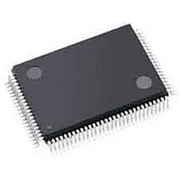
LFXP3C-3TN100I Lattice, LFXP3C-3TN100I Datasheet - Page 190

LFXP3C-3TN100I
Manufacturer Part Number
LFXP3C-3TN100I
Description
FPGA - Field Programmable Gate Array 3.1K LUTs 62 IO 1.8/ 2.5/3.3V -3 Spd I
Manufacturer
Lattice
Specifications of LFXP3C-3TN100I
Number Of Programmable I/os
62
Data Ram Size
55296
Supply Voltage (max)
3.465 V
Maximum Operating Temperature
+ 100 C
Minimum Operating Temperature
- 40 C
Mounting Style
SMD/SMT
Supply Voltage (min)
1.71 V
Package / Case
TQFP-100
Package
100TQFP
Family Name
LatticeXP
Device Logic Units
3000
Maximum Internal Frequency
320 MHz
Typical Operating Supply Voltage
1.8|2.5|3.3 V
Maximum Number Of User I/os
62
Ram Bits
55296
Re-programmability Support
Yes
Lead Free Status / RoHS Status
Lead free / RoHS Compliant
Available stocks
Company
Part Number
Manufacturer
Quantity
Price
Company:
Part Number:
LFXP3C-3TN100I
Manufacturer:
Lattice Semiconductor Corporation
Quantity:
10 000
- Current page: 190 of 397
- Download datasheet (10Mb)
Lattice Semiconductor
Figure 9-26. PSEUDO DUAL PORT RAM Timing Diagram – with Output Registers
Read Only Memory (ROM) – EBR Based
The EBR blocks in the LatticeECP/EC and LatticeXP devices can be configured as Read Only Memory or ROM.
IPexpress allows users to generate the Verilog-HDL or VHDL along with an EDIF netlist for the memory size as per
design requirements. Users are required to provide the ROM memory content in the form of an initialization file.
IPexpress generates the memory module as shown in Figure 9-27.
Figure 9-27. ROM - Read Only Memory Module Generated by IPexpress
The generated module makes use of these EBR blocks or primitives. For memory sizes smaller than an EBR block,
the module will be created in one EBR block. If the specified memory is larger than one EBR block, multiple EBR
blocks can be cascaded, in depth or width (as required to create these sizes).
The basic ROM primitive for the LatticeECP/EC and LatticeXP devices is as shown in Figure 9-28.
WrClockEn
RdClockEn
WrAddress
RdAddress
WrClock
RdClock
Data
Q
t
t
SUADDR_EBR
SUADDR_EBR
t
SUDATA_EBR
t
SUCE_EBR
Data_0
Add_0
OutClockEn
t
t
t
OutClock
HADDR_EBR
HADDR_EBR
HDATA_EBR
Address
Reset
Data_1
Add_1
Invalid Data
EBR based Read Only
t
SUCE_EBR
9-25
Memory
ROM
Add_0
LatticeECP/EC and LatticeXP Devices
t
HCE_EBR
Q
Add_1
Memory Usage Guide
t
COO_EBR
Data_2
Add_2
Data_0
Add_2
t
HCE_EBR
Dat
a_1
Related parts for LFXP3C-3TN100I
Image
Part Number
Description
Manufacturer
Datasheet
Request
R

Part Number:
Description:
FPGA - Field Programmable Gate Array 3.1K LUTs 136 IO 1.8 /2.5/3.3V -3 Spd I
Manufacturer:
Lattice

Part Number:
Description:
FPGA - Field Programmable Gate Array 3.1K LUTs 62 IO 1.8/ 2.5/3.3V -3 Spd I
Manufacturer:
Lattice

Part Number:
Description:
FPGA - Field Programmable Gate Array 3.1K LUTs 136 IO 1.8 /2.5/3.3V -3 Spd
Manufacturer:
Lattice

Part Number:
Description:
FPGA - Field Programmable Gate Array 3.1K LUTs 100 I/O 1.8/2.5/3.3V -3 Spd
Manufacturer:
Lattice
Datasheet:

Part Number:
Description:
FPGA - Field Programmable Gate Array 3.1K LUTS 100 I/O
Manufacturer:
Lattice
Datasheet:

Part Number:
Description:
FPGA - Field Programmable Gate Array 3.1K LUTS 136 I/O
Manufacturer:
Lattice
Datasheet:

Part Number:
Description:
FPGA - Field Programmable Gate Array 3.1K LUTs 100 I/O 1.8/2.5/3.3V -4 Spd
Manufacturer:
Lattice
Datasheet:

Part Number:
Description:
FPGA - Field Programmable Gate Array 3.1K LUTS 62 I/O
Manufacturer:
Lattice
Datasheet:

Part Number:
Description:
FPGA - Field Programmable Gate Array 3.1K LUTs 62 I/O 1.8/2.5/3.3V -4 Spd
Manufacturer:
Lattice
Datasheet:

Part Number:
Description:
FPGA - Field Programmable Gate Array 3.1K LUTS 62 I/O
Manufacturer:
Lattice
Datasheet:

Part Number:
Description:
FPGA - Field Programmable Gate Array 3.1K LUTs 100 I/O 1.8/2.5/3.3V IND
Manufacturer:
Lattice
Datasheet:

Part Number:
Description:
FPGA, 1.8V FLASH, INSTANT ON, SMD
Manufacturer:
LATTICE SEMICONDUCTOR
Datasheet:
Part Number:
Description:
FPGA LatticeXP Family 3000 Cells 320MHz 130nm (CMOS) Technology 1.8V/2.5V/3.3V 208-Pin PQFP Tray
Manufacturer:
LATTICE SEMICONDUCTOR
Datasheet:
Part Number:
Description:
FPGA LatticeXP Family 3000 Cells 320MHz 130nm (CMOS) Technology 1.8V/2.5V/3.3V 144-Pin TQFP Tray
Manufacturer:
LATTICE SEMICONDUCTOR
Datasheet:
Part Number:
Description:
FPGA LatticeXP Family 3000 Cells 360MHz 130nm (CMOS) Technology 1.8V/2.5V/3.3V 100-Pin TQFP Tray
Manufacturer:
LATTICE SEMICONDUCTOR
Datasheet:


