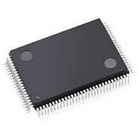
LFXP3C-3TN100I Lattice, LFXP3C-3TN100I Datasheet - Page 231

LFXP3C-3TN100I
Manufacturer Part Number
LFXP3C-3TN100I
Description
FPGA - Field Programmable Gate Array 3.1K LUTs 62 IO 1.8/ 2.5/3.3V -3 Spd I
Manufacturer
Lattice
Specifications of LFXP3C-3TN100I
Number Of Programmable I/os
62
Data Ram Size
55296
Supply Voltage (max)
3.465 V
Maximum Operating Temperature
+ 100 C
Minimum Operating Temperature
- 40 C
Mounting Style
SMD/SMT
Supply Voltage (min)
1.71 V
Package / Case
TQFP-100
Package
100TQFP
Family Name
LatticeXP
Device Logic Units
3000
Maximum Internal Frequency
320 MHz
Typical Operating Supply Voltage
1.8|2.5|3.3 V
Maximum Number Of User I/os
62
Ram Bits
55296
Re-programmability Support
Yes
Lead Free Status / RoHS Status
Lead free / RoHS Compliant
Available stocks
Company
Part Number
Manufacturer
Quantity
Price
Company:
Part Number:
LFXP3C-3TN100I
Manufacturer:
Lattice Semiconductor Corporation
Quantity:
10 000
- Current page: 231 of 397
- Download datasheet (10Mb)
Lattice Semiconductor
Figure 10-13. Read Data Transfer When DDRCLKPOL=1
Data Read Critical Path
Data in the second stage DDR registers can be registered either on the positive edge or on the falling edge of
FPGA clock depending on the DDRCLKPOL signal. In order to ensure that the data transferred to the FPGA core
registers is aligned to the rising edge of system CLK, this path should be constrained with a half clock transfer. This
half clock transfer can be forced in the software by assigning a multicycle constraint (multicycle of 0.5 X) on all the
data paths to the first PFU register.
Notes -
(1) DDR memory sends DQ aligned to DQS strobe.
(2) The DQS Strobe is delayed by 90 degree using the dedicated DQS logic.
(3) DQ is now center aligned to DQS Strobe.
(4) PRMBDET is the Preamble detect signal generated using the DQSBUFB primitive. This is used to
(5) The first set of IO registers A and B, capture data on the positive edge and negative edge of DQS.
(6) IO register C transfers data so that both data are now aligned to negative edge of DQS.
(7) DDCLKPOL signal generated will determine if the CLK going into the synchronization registers need to
(8) The IO Synchronization registers capture data at on negative edge of the FPGA CLK.
DDRCLKPOL=1
IO REGISTERS
CLK TO SYNC
generate the DDRCLKPOL signal.
be inverted. In this case, the DDRCLKPOL=1 as the CLK is HIGH at the 1
DQS at PIN
DQS at IOL
PRMBDET
FPGA CLK
DATAIN_P
DATAIN_N
DQ at PIN
DQ at IOL
C
A
B
P0
P0
10-12
N0
N0
P0
P1
P1
N0
P0
N1
P1
N1
P0
N0
st
LatticeECP/EC and LatticeXP
N1
P1
rising edge of PRMBDET.
DDR Usage Guide
Related parts for LFXP3C-3TN100I
Image
Part Number
Description
Manufacturer
Datasheet
Request
R

Part Number:
Description:
FPGA - Field Programmable Gate Array 3.1K LUTs 136 IO 1.8 /2.5/3.3V -3 Spd I
Manufacturer:
Lattice

Part Number:
Description:
FPGA - Field Programmable Gate Array 3.1K LUTs 62 IO 1.8/ 2.5/3.3V -3 Spd I
Manufacturer:
Lattice

Part Number:
Description:
FPGA - Field Programmable Gate Array 3.1K LUTs 136 IO 1.8 /2.5/3.3V -3 Spd
Manufacturer:
Lattice

Part Number:
Description:
FPGA - Field Programmable Gate Array 3.1K LUTs 100 I/O 1.8/2.5/3.3V -3 Spd
Manufacturer:
Lattice
Datasheet:

Part Number:
Description:
FPGA - Field Programmable Gate Array 3.1K LUTS 100 I/O
Manufacturer:
Lattice
Datasheet:

Part Number:
Description:
FPGA - Field Programmable Gate Array 3.1K LUTS 136 I/O
Manufacturer:
Lattice
Datasheet:

Part Number:
Description:
FPGA - Field Programmable Gate Array 3.1K LUTs 100 I/O 1.8/2.5/3.3V -4 Spd
Manufacturer:
Lattice
Datasheet:

Part Number:
Description:
FPGA - Field Programmable Gate Array 3.1K LUTS 62 I/O
Manufacturer:
Lattice
Datasheet:

Part Number:
Description:
FPGA - Field Programmable Gate Array 3.1K LUTs 62 I/O 1.8/2.5/3.3V -4 Spd
Manufacturer:
Lattice
Datasheet:

Part Number:
Description:
FPGA - Field Programmable Gate Array 3.1K LUTS 62 I/O
Manufacturer:
Lattice
Datasheet:

Part Number:
Description:
FPGA - Field Programmable Gate Array 3.1K LUTs 100 I/O 1.8/2.5/3.3V IND
Manufacturer:
Lattice
Datasheet:

Part Number:
Description:
FPGA, 1.8V FLASH, INSTANT ON, SMD
Manufacturer:
LATTICE SEMICONDUCTOR
Datasheet:
Part Number:
Description:
FPGA LatticeXP Family 3000 Cells 320MHz 130nm (CMOS) Technology 1.8V/2.5V/3.3V 208-Pin PQFP Tray
Manufacturer:
LATTICE SEMICONDUCTOR
Datasheet:
Part Number:
Description:
FPGA LatticeXP Family 3000 Cells 320MHz 130nm (CMOS) Technology 1.8V/2.5V/3.3V 144-Pin TQFP Tray
Manufacturer:
LATTICE SEMICONDUCTOR
Datasheet:
Part Number:
Description:
FPGA LatticeXP Family 3000 Cells 360MHz 130nm (CMOS) Technology 1.8V/2.5V/3.3V 100-Pin TQFP Tray
Manufacturer:
LATTICE SEMICONDUCTOR
Datasheet:


