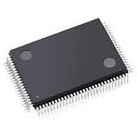
LFXP3C-3TN100I Lattice, LFXP3C-3TN100I Datasheet - Page 337

LFXP3C-3TN100I
Manufacturer Part Number
LFXP3C-3TN100I
Description
FPGA - Field Programmable Gate Array 3.1K LUTs 62 IO 1.8/ 2.5/3.3V -3 Spd I
Manufacturer
Lattice
Specifications of LFXP3C-3TN100I
Number Of Programmable I/os
62
Data Ram Size
55296
Supply Voltage (max)
3.465 V
Maximum Operating Temperature
+ 100 C
Minimum Operating Temperature
- 40 C
Mounting Style
SMD/SMT
Supply Voltage (min)
1.71 V
Package / Case
TQFP-100
Package
100TQFP
Family Name
LatticeXP
Device Logic Units
3000
Maximum Internal Frequency
320 MHz
Typical Operating Supply Voltage
1.8|2.5|3.3 V
Maximum Number Of User I/os
62
Ram Bits
55296
Re-programmability Support
Yes
Lead Free Status / RoHS Status
Lead free / RoHS Compliant
Available stocks
Company
Part Number
Manufacturer
Quantity
Price
Company:
Part Number:
LFXP3C-3TN100I
Manufacturer:
Lattice Semiconductor Corporation
Quantity:
10 000
- Current page: 337 of 397
- Download datasheet (10Mb)
Lattice Semiconductor
Implementing Multiplexers
The flexible configurations of LUTs can realize any 4-, 5-, or 6-input logic function like 2-to-1, 3-to-1 or 4-to-1 multi-
plexers. Larger multiplexers can be efficiently created by programming multiple 4-input LUTs. Synthesis tools camn
automatically infer Lattice FPGA optimized multiplexer library elements based on the behavioral description in the
HDL source code. This provides the flexibility to the Mapper and Place and Route tools to configure the LUT mode
and connections in the most optimum fashion.
Clock Dividers
There are two ways to implement clock dividers in Lattice Semiconductor FPGA devices. The first is to cascade the
registers with asynchronous clocks. The register output feeds the clock pin of the next register (Figure 13-7). Since
the clock number in each PFU is limited to two, any clock divider with more than two bits will require multiple PFU
implementations. As a result, the asynchronous daisy chaining implementation of clock divider will be slower due to
the inter-PFU routing delays. This kind of delays is usually ambiguous and inconsistent because of the nature of
FPGA routing structures.
Figure 13-7. Daisy Chaining of Flip-flops
16:1 MUX
…
process(sel, din)
…
LU
D
begin
end process;
if
elsif (sel="0001") then muxout <= din(1);
elsif (sel="0010") then muxout <= din(2);
elsif (sel="0011") then muxout <= din(3);
elsif (sel="0100") then muxout <= din(4);
elsif (sel="0101") then muxout <= din(5);
elsif (sel="0110") then muxout <= din(6);
elsif (sel="0111") then muxout <= din(7);
elsif (sel="1000") then muxout <= din(8);
elsif (sel="1001") then muxout <= din(9);
elsif (sel="1010") then muxout <= din(10);
elsif (sel="1011") then muxout <= din(11);
elsif (sel="1100") then muxout <= din(12);
elsif (sel="1101") then muxout <= din(13);
elsif (sel="1110") then muxout <= din(14);
elsif (sel="1111") then muxout <= din(15);
else muxout <= '0';
end if;
PFU
(sel="0000") then muxout <= din(0);
13-10
LU
D
PFU
HDL Synthesis Coding Guidelines
for Lattice Semiconductor FPGAs
Related parts for LFXP3C-3TN100I
Image
Part Number
Description
Manufacturer
Datasheet
Request
R

Part Number:
Description:
FPGA - Field Programmable Gate Array 3.1K LUTs 136 IO 1.8 /2.5/3.3V -3 Spd I
Manufacturer:
Lattice

Part Number:
Description:
FPGA - Field Programmable Gate Array 3.1K LUTs 62 IO 1.8/ 2.5/3.3V -3 Spd I
Manufacturer:
Lattice

Part Number:
Description:
FPGA - Field Programmable Gate Array 3.1K LUTs 136 IO 1.8 /2.5/3.3V -3 Spd
Manufacturer:
Lattice

Part Number:
Description:
FPGA - Field Programmable Gate Array 3.1K LUTs 100 I/O 1.8/2.5/3.3V -3 Spd
Manufacturer:
Lattice
Datasheet:

Part Number:
Description:
FPGA - Field Programmable Gate Array 3.1K LUTS 100 I/O
Manufacturer:
Lattice
Datasheet:

Part Number:
Description:
FPGA - Field Programmable Gate Array 3.1K LUTS 136 I/O
Manufacturer:
Lattice
Datasheet:

Part Number:
Description:
FPGA - Field Programmable Gate Array 3.1K LUTs 100 I/O 1.8/2.5/3.3V -4 Spd
Manufacturer:
Lattice
Datasheet:

Part Number:
Description:
FPGA - Field Programmable Gate Array 3.1K LUTS 62 I/O
Manufacturer:
Lattice
Datasheet:

Part Number:
Description:
FPGA - Field Programmable Gate Array 3.1K LUTs 62 I/O 1.8/2.5/3.3V -4 Spd
Manufacturer:
Lattice
Datasheet:

Part Number:
Description:
FPGA - Field Programmable Gate Array 3.1K LUTS 62 I/O
Manufacturer:
Lattice
Datasheet:

Part Number:
Description:
FPGA - Field Programmable Gate Array 3.1K LUTs 100 I/O 1.8/2.5/3.3V IND
Manufacturer:
Lattice
Datasheet:

Part Number:
Description:
FPGA, 1.8V FLASH, INSTANT ON, SMD
Manufacturer:
LATTICE SEMICONDUCTOR
Datasheet:
Part Number:
Description:
FPGA LatticeXP Family 3000 Cells 320MHz 130nm (CMOS) Technology 1.8V/2.5V/3.3V 208-Pin PQFP Tray
Manufacturer:
LATTICE SEMICONDUCTOR
Datasheet:
Part Number:
Description:
FPGA LatticeXP Family 3000 Cells 320MHz 130nm (CMOS) Technology 1.8V/2.5V/3.3V 144-Pin TQFP Tray
Manufacturer:
LATTICE SEMICONDUCTOR
Datasheet:
Part Number:
Description:
FPGA LatticeXP Family 3000 Cells 360MHz 130nm (CMOS) Technology 1.8V/2.5V/3.3V 100-Pin TQFP Tray
Manufacturer:
LATTICE SEMICONDUCTOR
Datasheet:


