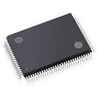
LFXP3C-3TN100I Lattice, LFXP3C-3TN100I Datasheet - Page 348

LFXP3C-3TN100I
Manufacturer Part Number
LFXP3C-3TN100I
Description
FPGA - Field Programmable Gate Array 3.1K LUTs 62 IO 1.8/ 2.5/3.3V -3 Spd I
Manufacturer
Lattice
Specifications of LFXP3C-3TN100I
Number Of Programmable I/os
62
Data Ram Size
55296
Supply Voltage (max)
3.465 V
Maximum Operating Temperature
+ 100 C
Minimum Operating Temperature
- 40 C
Mounting Style
SMD/SMT
Supply Voltage (min)
1.71 V
Package / Case
TQFP-100
Package
100TQFP
Family Name
LatticeXP
Device Logic Units
3000
Maximum Internal Frequency
320 MHz
Typical Operating Supply Voltage
1.8|2.5|3.3 V
Maximum Number Of User I/os
62
Ram Bits
55296
Re-programmability Support
Yes
Lead Free Status / RoHS Status
Lead free / RoHS Compliant
Available stocks
Company
Part Number
Manufacturer
Quantity
Price
Company:
Part Number:
LFXP3C-3TN100I
Manufacturer:
Lattice Semiconductor Corporation
Quantity:
10 000
- Current page: 348 of 397
- Download datasheet (10Mb)
Lattice Semiconductor
This particular example shows a 99.0% coverage. The way to find unconstrained paths is to run Trace with the
“Check Unconstrained Paths” checkbox selected. This will give a list of all of the signals that are not covered under
timing analysis. In some designs, many of these signals are a common ground net that indeed does not need to be
constrained. Designers should understand this point and use Trace (the ispLEVER static timing analysis tool) to
check unconstrained paths to make sure they are not missing any design paths that are timing critical.
Also, note the timing score shown in Figure 17-1. The timing score shows the total amount of error (in picoseconds)
for all timing preferences constraining the design. PAR attempts to minimize the timing score, PAR does not
attempt to maximize frequency.
The above discussion can be summarized by the following single equality:
Translating Board Requirements into FPGA Preferences
Understanding the system board level timing and design constraints is the primary requirement for producing a
complete preference file. As a result, the major requirements such as clock frequency, I/O timing and loads can be
translated into the appropriate preference statements in a constraint file.
The following exercise will provide an example on how to extract preferences from system conditions.
Figure 17-2 shows an example system involving the interface between a port controller and a Lattice Semiconduc-
tor FPGA.
Figure 17-2. Interface Timing Example
In the system above, several parameters have already been provided:
• System clock frequency: period (P): 30 ns.
• Port controller maximum output propagation delay (PDMAXp): 18ns.
• Port controller minimum output propagation delay (PDMINp): 3 ns.
• Port controller input setup specification (TSp): 5 ns.
• Port controller input hold specification (THp): 3 ns.
• Max board propagation delay (PDMAXb): 6 ns.
• Min board propagation delay (PDMINb): 1 ns.
• Port controller to FPGA device clock skew and vice versa (Tskew): 1 ns.
clk
Quality of Preference File = Quality of PAR Results
Chip to chip clock skew of 1 ns
Controller
3 ns to 18 ns clk to out,
5 ns setup, 3 ns hold
9 pf input capacitance,
60 pf AC load
Port
Board propagation
delay of 1 ns to 2 ns
PCB traces
17-4
5 pf parasitic board capacitance
Lattice
9 pf input capacitance
FPGA
Lattice Semiconductor FPGA
Successful Place and Route
Related parts for LFXP3C-3TN100I
Image
Part Number
Description
Manufacturer
Datasheet
Request
R

Part Number:
Description:
FPGA - Field Programmable Gate Array 3.1K LUTs 136 IO 1.8 /2.5/3.3V -3 Spd I
Manufacturer:
Lattice

Part Number:
Description:
FPGA - Field Programmable Gate Array 3.1K LUTs 62 IO 1.8/ 2.5/3.3V -3 Spd I
Manufacturer:
Lattice

Part Number:
Description:
FPGA - Field Programmable Gate Array 3.1K LUTs 136 IO 1.8 /2.5/3.3V -3 Spd
Manufacturer:
Lattice

Part Number:
Description:
FPGA - Field Programmable Gate Array 3.1K LUTs 100 I/O 1.8/2.5/3.3V -3 Spd
Manufacturer:
Lattice
Datasheet:

Part Number:
Description:
FPGA - Field Programmable Gate Array 3.1K LUTS 100 I/O
Manufacturer:
Lattice
Datasheet:

Part Number:
Description:
FPGA - Field Programmable Gate Array 3.1K LUTS 136 I/O
Manufacturer:
Lattice
Datasheet:

Part Number:
Description:
FPGA - Field Programmable Gate Array 3.1K LUTs 100 I/O 1.8/2.5/3.3V -4 Spd
Manufacturer:
Lattice
Datasheet:

Part Number:
Description:
FPGA - Field Programmable Gate Array 3.1K LUTS 62 I/O
Manufacturer:
Lattice
Datasheet:

Part Number:
Description:
FPGA - Field Programmable Gate Array 3.1K LUTs 62 I/O 1.8/2.5/3.3V -4 Spd
Manufacturer:
Lattice
Datasheet:

Part Number:
Description:
FPGA - Field Programmable Gate Array 3.1K LUTS 62 I/O
Manufacturer:
Lattice
Datasheet:

Part Number:
Description:
FPGA - Field Programmable Gate Array 3.1K LUTs 100 I/O 1.8/2.5/3.3V IND
Manufacturer:
Lattice
Datasheet:

Part Number:
Description:
FPGA, 1.8V FLASH, INSTANT ON, SMD
Manufacturer:
LATTICE SEMICONDUCTOR
Datasheet:
Part Number:
Description:
FPGA LatticeXP Family 3000 Cells 320MHz 130nm (CMOS) Technology 1.8V/2.5V/3.3V 208-Pin PQFP Tray
Manufacturer:
LATTICE SEMICONDUCTOR
Datasheet:
Part Number:
Description:
FPGA LatticeXP Family 3000 Cells 320MHz 130nm (CMOS) Technology 1.8V/2.5V/3.3V 144-Pin TQFP Tray
Manufacturer:
LATTICE SEMICONDUCTOR
Datasheet:
Part Number:
Description:
FPGA LatticeXP Family 3000 Cells 360MHz 130nm (CMOS) Technology 1.8V/2.5V/3.3V 100-Pin TQFP Tray
Manufacturer:
LATTICE SEMICONDUCTOR
Datasheet:


