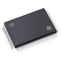
LFXP3C-3TN100I Lattice, LFXP3C-3TN100I Datasheet - Page 232

LFXP3C-3TN100I
Manufacturer Part Number
LFXP3C-3TN100I
Description
FPGA - Field Programmable Gate Array 3.1K LUTs 62 IO 1.8/ 2.5/3.3V -3 Spd I
Manufacturer
Lattice
Specifications of LFXP3C-3TN100I
Number Of Programmable I/os
62
Data Ram Size
55296
Supply Voltage (max)
3.465 V
Maximum Operating Temperature
+ 100 C
Minimum Operating Temperature
- 40 C
Mounting Style
SMD/SMT
Supply Voltage (min)
1.71 V
Package / Case
TQFP-100
Package
100TQFP
Family Name
LatticeXP
Device Logic Units
3000
Maximum Internal Frequency
320 MHz
Typical Operating Supply Voltage
1.8|2.5|3.3 V
Maximum Number Of User I/os
62
Ram Bits
55296
Re-programmability Support
Yes
Lead Free Status / RoHS Status
Lead free / RoHS Compliant
Available stocks
Company
Part Number
Manufacturer
Quantity
Price
Company:
Part Number:
LFXP3C-3TN100I
Manufacturer:
Lattice Semiconductor Corporation
Quantity:
10 000
- Current page: 232 of 397
- Download datasheet (10Mb)
Lattice Semiconductor
DQS Postamble
At the end of a READ cycle, the DDR SDRAM device executes the READ cycle postamble and then immediately
tristates both the DQ and DQS output drivers. Since neither the memory controller (FPGA) nor the DDR SDRAM
device are driving DQ or DQS at that time, these signals float to a level determined by the off-chip termination
resistors. While these signals are floating, noise on the DQS strobe may be interpreted as a valid strobe signal by
the FPGA input buffer. This can cause the last READ data captured in the IOL input DDR registers to be overwrit-
ten before the data has been transferred to the free running resynchronization registers inside the FPGA.
Figure 10-14. Postamble Effect on READ
LatticeECP/EC and LatticeXP devices have extra dedicated logic in the in the DQS Delay Block that will prevent
this postamble problem. The DQS postamble logic is automatically implemented when the user instantiates the
DQS Delay logic (DQSBUFB software primitive) in a design.
This postamble solution was implemented in all the devices of the LatticeECP/EC and LatticeXP families except
the LFEC20/LFECP20 device. For this device, it is recommended that the user issue an extra READ command to
assure correct data has been transferred to the synchronization registers.
The circumstances under which the extended READ cycle is issued are given in Table 10-8.
Table 10-8. DDR Read Postamble
Read (Row x, Bank y)
Read (any address)
Read (Row x, Bank y)
Read (Row x, Bank y)
Read (any address)
1. Current read is extended one or more additional clock cycles.
Current Command
Read (Row x, Bank y)
NOP
Read (Row n, Bank y)
Read (Row x, Bank n)
Write/LMR
DQS at PIN
DQS at IOL
DATAIN_N
DATAIN_P
DQ at PIN
DQ at IOL
synce reg
Next Command
CLK at
C
A
B
None.
Extend the current read command.
Extend the current read to (Row x, Bank y) consecutive to
current command
If the Row x, Bank n was open, do nothing. Else, extend
the current read to Row x, Bank y
Extend the current read command.
P0
P0
10-13
P0
N0
N0
P1
P1
Action
N0
P0
P0
N0
P1
N1
N1
1
LatticeECP/EC and LatticeXP
N1
P1
DDR Usage Guide
Lost Cycles
None
3
3
3
3
Related parts for LFXP3C-3TN100I
Image
Part Number
Description
Manufacturer
Datasheet
Request
R

Part Number:
Description:
FPGA - Field Programmable Gate Array 3.1K LUTs 136 IO 1.8 /2.5/3.3V -3 Spd I
Manufacturer:
Lattice

Part Number:
Description:
FPGA - Field Programmable Gate Array 3.1K LUTs 62 IO 1.8/ 2.5/3.3V -3 Spd I
Manufacturer:
Lattice

Part Number:
Description:
FPGA - Field Programmable Gate Array 3.1K LUTs 136 IO 1.8 /2.5/3.3V -3 Spd
Manufacturer:
Lattice

Part Number:
Description:
FPGA - Field Programmable Gate Array 3.1K LUTs 100 I/O 1.8/2.5/3.3V -3 Spd
Manufacturer:
Lattice
Datasheet:

Part Number:
Description:
FPGA - Field Programmable Gate Array 3.1K LUTS 100 I/O
Manufacturer:
Lattice
Datasheet:

Part Number:
Description:
FPGA - Field Programmable Gate Array 3.1K LUTS 136 I/O
Manufacturer:
Lattice
Datasheet:

Part Number:
Description:
FPGA - Field Programmable Gate Array 3.1K LUTs 100 I/O 1.8/2.5/3.3V -4 Spd
Manufacturer:
Lattice
Datasheet:

Part Number:
Description:
FPGA - Field Programmable Gate Array 3.1K LUTS 62 I/O
Manufacturer:
Lattice
Datasheet:

Part Number:
Description:
FPGA - Field Programmable Gate Array 3.1K LUTs 62 I/O 1.8/2.5/3.3V -4 Spd
Manufacturer:
Lattice
Datasheet:

Part Number:
Description:
FPGA - Field Programmable Gate Array 3.1K LUTS 62 I/O
Manufacturer:
Lattice
Datasheet:

Part Number:
Description:
FPGA - Field Programmable Gate Array 3.1K LUTs 100 I/O 1.8/2.5/3.3V IND
Manufacturer:
Lattice
Datasheet:

Part Number:
Description:
FPGA, 1.8V FLASH, INSTANT ON, SMD
Manufacturer:
LATTICE SEMICONDUCTOR
Datasheet:
Part Number:
Description:
FPGA LatticeXP Family 3000 Cells 320MHz 130nm (CMOS) Technology 1.8V/2.5V/3.3V 208-Pin PQFP Tray
Manufacturer:
LATTICE SEMICONDUCTOR
Datasheet:
Part Number:
Description:
FPGA LatticeXP Family 3000 Cells 320MHz 130nm (CMOS) Technology 1.8V/2.5V/3.3V 144-Pin TQFP Tray
Manufacturer:
LATTICE SEMICONDUCTOR
Datasheet:
Part Number:
Description:
FPGA LatticeXP Family 3000 Cells 360MHz 130nm (CMOS) Technology 1.8V/2.5V/3.3V 100-Pin TQFP Tray
Manufacturer:
LATTICE SEMICONDUCTOR
Datasheet:


