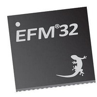
EFM32TG210F32 Energy Micro, EFM32TG210F32 Datasheet - Page 431

EFM32TG210F32
Manufacturer Part Number
EFM32TG210F32
Description
MCU 32BIT 32KB FLASH 32-QFN
Manufacturer
Energy Micro
Series
Tiny Geckor
Specifications of EFM32TG210F32
Core Processor
ARM® Cortex-M3™
Core Size
32-Bit
Speed
32MHz
Connectivity
EBI/EMI, I²C, IrDA, SmartCard, SPI, UART/USART
Peripherals
Brown-out Detect/Reset, DMA, POR, PWM, WDT
Number Of I /o
24
Program Memory Size
32KB (32K x 8)
Program Memory Type
FLASH
Ram Size
4K x 8
Voltage - Supply (vcc/vdd)
1.8 V ~ 3.8 V
Data Converters
A/D 4x12b, D/A 1x12b
Oscillator Type
External
Operating Temperature
-40°C ~ 85°C
Package / Case
32-VQFN Exposed Pad
Processor Series
EFM32
Core
ARM Cortex-M3
Data Bus Width
32 bit
Data Ram Size
32 KB
Interface Type
UART, I2C, SPI
Maximum Clock Frequency
32 MHz
Number Of Programmable I/os
17
Number Of Timers
1
Operating Supply Voltage
1.8 V to 3.8 V
Maximum Operating Temperature
+ 85 C
Mounting Style
SMD/SMT
Processor To Be Evaluated
EFM32TG210
Lead Free Status / RoHS Status
Lead free / RoHS Compliant
Eeprom Size
-
Lead Free Status / Rohs Status
Details
- Current page: 431 of 522
- Download datasheet (9Mb)
26.3.2.5 Cascaded Inverting PGA
2010-12-21 - d0034_Rev0.90
the OPAxPOSSEL bitfield, and the output is configured by the OUTPEN bitfield, both located in
DACn_OPAxMUX.
Figure 26.5. Non-inverting PGA Overview
Table 26.4. Non-inverting PGA Configuration
This mode enables the opamp signals to be internally configured to cascade two or three opamp in
inverting mode as shown in Figure 26.6 (p. 431) . In both cases the positive input will be configured
to signal ground by setting OPAxPOSSEL bitfield to PAD in DACn_OPAx_MUX. When cascaded, the
negative input is connected to the resistor ladder by setting the OPAxNEGSEL bitfield to OPATAP in
DACn_OPAxMUX. The input to the resistor ladder can be configured in the OPAxRESINMUX bitfield
in DAC_nOPAxMUX. The output from OPA0 can be connected to OPA1 to create the second stage
by setting the NEXTOUT bitfield in DACn_OPAxMUX. To complete the stage, OPA1RESINMUX field
must be set to OPA0INP. Similarly, the last stage can be created by setting the NEXTOUT bitfield in
DACn_OPA1MUX and OPA2RESINMUX bitfield to OPA1INP in DACn_OPA2MUX.
Figure 26.6. Cascaded Inverting PGA Overview
Table 26.5. Cascaded Inverting PGA Configuration
VIN
OPA bitfields
OPAx POSSEL
OPAx NEGSEL
OPAx RESINMUX
OPA
OPA0
OPA0
OPA0
OPA0
OPA1
OPA1
POS0
R1
R1
VIN
+
-
R2
+
-
VOUT1= -(VIN-POS0) x R2/R1 + POS0
R2
POS1
R1
+
-
VOUT= VIN(1+ R2/R1)
R2
VOUT
OPA bitfields
POSSEL
NEGSEL
RESINMUX
OUTPEN
POSSEL
NEGSEL
VOUT2= -(VOUT1-POS1) x R2/R1 + POS1
POS2
R1
...the world's most energy friendly microcontrollers
431
+
-
R2
OPA Configuration
NEXTOUT, POSPADx, DACx
OPATAP
VSS, NEGPAD
VOUT3= -(VOUT2-POS3) x R2/R1 + POS3
OPA Configuration
POSPAD0
OPA0TAP
NEGPAD0
NEXTOUT
POSPAD1
OPATAP
www.energymicro.com
Related parts for EFM32TG210F32
Image
Part Number
Description
Manufacturer
Datasheet
Request
R

Part Number:
Description:
KIT STARTER EFM32 GECKO
Manufacturer:
Energy Micro
Datasheet:

Part Number:
Description:
KIT DEV EFM32 GECKO LCD SUPPORT
Manufacturer:
Energy Micro
Datasheet:

Part Number:
Description:
BOARD PROTOTYPING FOR EFM32
Manufacturer:
Energy Micro
Datasheet:

Part Number:
Description:
KIT DEVELOPMENT EFM32 GECKO
Manufacturer:
Energy Micro
Datasheet:

Part Number:
Description:
MCU, MPU & DSP Development Tools TG840 Sample Kit
Manufacturer:
Energy Micro
Datasheet:

Part Number:
Description:
MCU, MPU & DSP Development Tools TG Starter Kit
Manufacturer:
Energy Micro
Datasheet:

Part Number:
Description:
MCU, MPU & DSP Development Tools TG108 Sample Kit
Manufacturer:
Energy Micro

Part Number:
Description:
MCU, MPU & DSP Development Tools TG210 Sample Kit
Manufacturer:
Energy Micro
Datasheet:

Part Number:
Description:
MCU, MPU & DSP Development Tools TG822 Sample Kit
Manufacturer:
Energy Micro
Datasheet:

Part Number:
Description:
MCU, MPU & DSP Development Tools TG230 Sample Kit
Manufacturer:
Energy Micro

Part Number:
Description:
SAMPLE KIT (SMALL BOX - CONTAINING 2 DEVICES)
Manufacturer:
Energy Micro

Part Number:
Description:
SAMPLE KIT (SMALL BOX - CONTAINING 2 DEVICES)
Manufacturer:
Energy Micro


