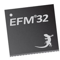
EFM32TG210F32 Energy Micro, EFM32TG210F32 Datasheet - Page 19

EFM32TG210F32
Manufacturer Part Number
EFM32TG210F32
Description
MCU 32BIT 32KB FLASH 32-QFN
Manufacturer
Energy Micro
Series
Tiny Geckor
Specifications of EFM32TG210F32
Core Processor
ARM® Cortex-M3™
Core Size
32-Bit
Speed
32MHz
Connectivity
EBI/EMI, I²C, IrDA, SmartCard, SPI, UART/USART
Peripherals
Brown-out Detect/Reset, DMA, POR, PWM, WDT
Number Of I /o
24
Program Memory Size
32KB (32K x 8)
Program Memory Type
FLASH
Ram Size
4K x 8
Voltage - Supply (vcc/vdd)
1.8 V ~ 3.8 V
Data Converters
A/D 4x12b, D/A 1x12b
Oscillator Type
External
Operating Temperature
-40°C ~ 85°C
Package / Case
32-VQFN Exposed Pad
Processor Series
EFM32
Core
ARM Cortex-M3
Data Bus Width
32 bit
Data Ram Size
32 KB
Interface Type
UART, I2C, SPI
Maximum Clock Frequency
32 MHz
Number Of Programmable I/os
17
Number Of Timers
1
Operating Supply Voltage
1.8 V to 3.8 V
Maximum Operating Temperature
+ 85 C
Mounting Style
SMD/SMT
Processor To Be Evaluated
EFM32TG210
Lead Free Status / RoHS Status
Lead free / RoHS Compliant
Eeprom Size
-
Lead Free Status / Rohs Status
Details
- Current page: 19 of 522
- Download datasheet (9Mb)
5.3.1.1.1 Delayed synchronization
5.3.1.1.2 Immediate synchronization
2010-12-21 - d0034_Rev0.90
clock on the Low Energy Peripheral being accessed. Registers requiring synchronization are marked
"Asynchronous in their description header.
Note
After writing data to a register which value is to be synchronized into the Low Energy Peripheral using
delayed synchronization, a corresponding busy flag in the <module_name>_SYNCBUSY register (e.g.
RTC_SYNCBUSY) is set. This flag is set as long as synchronization is in progress and is cleared upon
completion.
Note
See Figure 5.2 (p. 19) for an overview of the writing mechanism operation.
Figure 5.2. Write operation to Low Energy Peripherals
In contrast to the peripherals with delayed synchronization, peripherals with immediate synchronization
don't experience a delay from a value is written to it takes effect in the peripheral. They are updated
immediately on the peripheral write access. If such a write is done close to an edge on the clock of
the peripheral, the write is delayed to after the clock edge. This will introduce wait-states on peripheral
access.
On peripherals with delayed synchronization, the SYNCBUSY registers are still present. These have two
purposes: Commands written to a peripheral with immediate synchronization are not executed before the
first peripheral clock after the write. In this period, the SYNCBUSY flag for the command register is set,
indicating that the command has not yet been performed. The second reason is backwards compatibility.
To maintain compatibility with the Gecko series, the rest of the SYNCBUSY registers are also present,
but these are always 0, indicating that register writes are always safe.
Note
Write[ 0:n]
On the Gecko series of devices, all LE peripherals are subject to delayed synchronization.
Subsequent writes to the same register before the corresponding busy flag is cleared is not
supported. Write before the busy flag is cleared may result in undefined behavior.
In general the SYNCBUSY register only needs to be observed if there is a risk of multiple
write access to a register (which must be prevented). It is not required to wait until the
relevant flag in the SYNCBUSY register is cleared after writing a register. E.g can EM2 be
entered directly after writing a register.
Set 0
Set 1
Set n
Core Clock Dom ain
Core Clock
Syncbusy Register 0
Syncbusy Register 1
Syncbusy Register n
Register 0
Register 1
Register n
.
.
.
.
.
.
Clear 0
Clear 1
Clear n
Freeze
...the world's most energy friendly microcontrollers
19
Synchronization Done
Low Frequency Clock
Synchronizer 0
Synchronizer 1
Low Frequency Clock Dom ain
Synchronizer n
.
.
.
www.energymicro.com
Low Frequency Clock
Register 0 Sync
Register 1 Sync
Register n Sync
.
.
.
Related parts for EFM32TG210F32
Image
Part Number
Description
Manufacturer
Datasheet
Request
R

Part Number:
Description:
KIT STARTER EFM32 GECKO
Manufacturer:
Energy Micro
Datasheet:

Part Number:
Description:
KIT DEV EFM32 GECKO LCD SUPPORT
Manufacturer:
Energy Micro
Datasheet:

Part Number:
Description:
BOARD PROTOTYPING FOR EFM32
Manufacturer:
Energy Micro
Datasheet:

Part Number:
Description:
KIT DEVELOPMENT EFM32 GECKO
Manufacturer:
Energy Micro
Datasheet:

Part Number:
Description:
MCU, MPU & DSP Development Tools TG840 Sample Kit
Manufacturer:
Energy Micro
Datasheet:

Part Number:
Description:
MCU, MPU & DSP Development Tools TG Starter Kit
Manufacturer:
Energy Micro
Datasheet:

Part Number:
Description:
MCU, MPU & DSP Development Tools TG108 Sample Kit
Manufacturer:
Energy Micro

Part Number:
Description:
MCU, MPU & DSP Development Tools TG210 Sample Kit
Manufacturer:
Energy Micro
Datasheet:

Part Number:
Description:
MCU, MPU & DSP Development Tools TG822 Sample Kit
Manufacturer:
Energy Micro
Datasheet:

Part Number:
Description:
MCU, MPU & DSP Development Tools TG230 Sample Kit
Manufacturer:
Energy Micro

Part Number:
Description:
SAMPLE KIT (SMALL BOX - CONTAINING 2 DEVICES)
Manufacturer:
Energy Micro

Part Number:
Description:
SAMPLE KIT (SMALL BOX - CONTAINING 2 DEVICES)
Manufacturer:
Energy Micro


