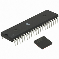
ATMEGA64RZAV-10PU Atmel, ATMEGA64RZAV-10PU Datasheet - Page 43

ATMEGA64RZAV-10PU
Manufacturer Part Number
ATMEGA64RZAV-10PU
Description
MCU ATMEGA644/AT86RF230 40-DIP
Manufacturer
Atmel
Series
ATMEGAr
Datasheets
1.ATMEGA644-20MU.pdf
(23 pages)
2.ATMEGA644-20MU.pdf
(376 pages)
3.AT86RF230-ZU.pdf
(98 pages)
Specifications of ATMEGA64RZAV-10PU
Frequency
2.4GHz
Modulation Or Protocol
802.15.4 Zigbee
Power - Output
3dBm
Sensitivity
-101dBm
Voltage - Supply
1.8 V ~ 3.6 V
Data Interface
PCB, Surface Mount
Memory Size
64kB Flash, 2kB EEPROM, 4kB RAM
Antenna Connector
PCB, Surface Mount
Package / Case
40-DIP (0.600", 15.24mm)
Wireless Frequency
2.4 GHz
Interface Type
JTAG, SPI
Output Power
3 dBm
For Use With
ATSTK600-TQFP32 - STK600 SOCKET/ADAPTER 32-TQFPATAVRISP2 - PROGRAMMER AVR IN SYSTEMATSTK500 - PROGRAMMER AVR STARTER KIT
Lead Free Status / RoHS Status
Lead free / RoHS Compliant
Operating Temperature
-
Applications
-
Data Rate - Maximum
-
Current - Transmitting
-
Current - Receiving
-
Lead Free Status / Rohs Status
Lead free / RoHS Compliant
For Use With/related Products
ATmega64
- Current page: 43 of 376
- Download datasheet (8Mb)
8.10.7
8.11
8.11.1
2593N–AVR–07/10
Register Description
On-chip Debug System
SMCR – Sleep Mode Control Register
DIDR0). Refer to
Input Disable Register 0” on page 252
If the On-chip debug system is enabled by the OCDEN Fuse and the chip enters sleep mode,
the main clock source is enabled, and hence, always consumes power. In the deeper sleep
modes, this will contribute significantly to the total current consumption.
There are three alternative ways to disable the OCD system:
• Disable the OCDEN Fuse.
• Disable the JTAGEN Fuse.
• Write one to the JTD bit in MCUCR.
The Sleep Mode Control Register contains control bits for power management.
• Bits 3, 2, 1 – SM2:0: Sleep Mode Select Bits 2, 1, and 0
These bits select between the five available sleep modes as shown in
Table 8-2.
Note:
• Bit 0 – SE: Sleep Enable
The SE bit must be written to logic one to make the MCU enter the sleep mode when the SLEEP
instruction is executed. To avoid the MCU entering the sleep mode unless it is the programmer’s
purpose, it is recommended to write the Sleep Enable (SE) bit to one just before the execution of
the SLEEP instruction and to clear it immediately after waking up.
Bit
0x33 (0x53)
Read/Write
Initial Value
SM2
0
0
0
0
1
1
1
1
1. Standby modes are only recommended for use with external crystals or resonators.
Sleep Mode Select
7
–
R
0
”DIDR1 – Digital Input Disable Register 1” on page 232
SM1
0
0
1
1
0
0
1
1
6
–
R
0
R
5
–
0
SM0
0
1
0
1
0
1
0
1
for details.
R
4
–
0
Sleep Mode
Idle
ADC Noise Reduction
Power-down
Power-save
Reserved
Reserved
Standby
Extended Standby
SM2
R/W
3
0
(1)
SM1
R/W
2
0
(1)
SM0
R/W
Table
1
0
ATmega644
and
8-2.
”DIDR0 – Digital
R/W
SE
0
0
SMCR
43
Related parts for ATMEGA64RZAV-10PU
Image
Part Number
Description
Manufacturer
Datasheet
Request
R

Part Number:
Description:
DEV KIT FOR AVR/AVR32
Manufacturer:
Atmel
Datasheet:

Part Number:
Description:
INTERVAL AND WIPE/WASH WIPER CONTROL IC WITH DELAY
Manufacturer:
ATMEL Corporation
Datasheet:

Part Number:
Description:
Low-Voltage Voice-Switched IC for Hands-Free Operation
Manufacturer:
ATMEL Corporation
Datasheet:

Part Number:
Description:
MONOLITHIC INTEGRATED FEATUREPHONE CIRCUIT
Manufacturer:
ATMEL Corporation
Datasheet:

Part Number:
Description:
AM-FM Receiver IC U4255BM-M
Manufacturer:
ATMEL Corporation
Datasheet:

Part Number:
Description:
Monolithic Integrated Feature Phone Circuit
Manufacturer:
ATMEL Corporation
Datasheet:

Part Number:
Description:
Multistandard Video-IF and Quasi Parallel Sound Processing
Manufacturer:
ATMEL Corporation
Datasheet:

Part Number:
Description:
High-performance EE PLD
Manufacturer:
ATMEL Corporation
Datasheet:

Part Number:
Description:
8-bit Flash Microcontroller
Manufacturer:
ATMEL Corporation
Datasheet:

Part Number:
Description:
2-Wire Serial EEPROM
Manufacturer:
ATMEL Corporation
Datasheet:


