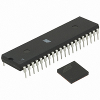
ATMEGA64RZAV-10PU Atmel, ATMEGA64RZAV-10PU Datasheet - Page 239

ATMEGA64RZAV-10PU
Manufacturer Part Number
ATMEGA64RZAV-10PU
Description
MCU ATMEGA644/AT86RF230 40-DIP
Manufacturer
Atmel
Series
ATMEGAr
Datasheets
1.ATMEGA644-20MU.pdf
(23 pages)
2.ATMEGA644-20MU.pdf
(376 pages)
3.AT86RF230-ZU.pdf
(98 pages)
Specifications of ATMEGA64RZAV-10PU
Frequency
2.4GHz
Modulation Or Protocol
802.15.4 Zigbee
Power - Output
3dBm
Sensitivity
-101dBm
Voltage - Supply
1.8 V ~ 3.6 V
Data Interface
PCB, Surface Mount
Memory Size
64kB Flash, 2kB EEPROM, 4kB RAM
Antenna Connector
PCB, Surface Mount
Package / Case
40-DIP (0.600", 15.24mm)
Wireless Frequency
2.4 GHz
Interface Type
JTAG, SPI
Output Power
3 dBm
For Use With
ATSTK600-TQFP32 - STK600 SOCKET/ADAPTER 32-TQFPATAVRISP2 - PROGRAMMER AVR IN SYSTEMATSTK500 - PROGRAMMER AVR STARTER KIT
Lead Free Status / RoHS Status
Lead free / RoHS Compliant
Operating Temperature
-
Applications
-
Data Rate - Maximum
-
Current - Transmitting
-
Current - Receiving
-
Lead Free Status / Rohs Status
Lead free / RoHS Compliant
For Use With/related Products
ATmega64
- Current page: 239 of 376
- Download datasheet (8Mb)
21.5.1
21.6
2593N–AVR–07/10
Changing Channel or Reference Selection
Differential Gain Channels
Table 21-1.
When using differential gain channels, certain aspects of the conversion need to be taken into
consideration.
Differential conversions are synchronized to the internal clock CK
clock. This synchronization is done automatically by the ADC interface in such a way that the
sample-and-hold occurs at a specific phase of CK
all single conversions, and the first free running conversion) when CK
same amount of time as a single ended conversion (13 ADC clock cycles from the next pres-
caled clock cycle). A conversion initiated by the user when CK
cycles due to the synchronization mechanism. In Free Running mode, a new conversion is initi-
ated immediately after the previous conversion completes, and since CK
all automatically started (that is, all but the first) free running conversions will take 14 ADC clock
cycles.
The gain stage is optimized for a bandwidth of 4 kHz at all gain settings. Higher frequencies may
be subjected to non-linear amplification. An external low-pass filter should be used if the input
signal contains higher frequency components than the gain stage bandwidth. Note that the ADC
clock frequency is independent of the gain stage bandwidth limitation. For example, the ADC
clock period may be 6 µs, allowing a channel to be sampled at 12 kSPS, regardless of the band-
width of this channel.
If differential gain channels are used and conversions are started by Auto Triggering, the ADC
must be switched off between conversions. When Auto Triggering is used, the ADC prescaler is
reset before the conversion is started. Since the gain stage is dependent of a stable ADC clock
prior to the conversion, this conversion will not be valid. By disabling and then re-enabling the
ADC between each conversion (writing ADEN in ADCSRA to “0” then to “1”), only extended con-
versions are performed. The result from the extended conversions will be valid. See
and Conversion Timing” on page 236
The MUXn and REFS1:0 bits in the ADMUX Register are single buffered through a temporary
register to which the CPU has random access. This ensures that the channels and reference
selection only takes place at a safe point during the conversion. The channel and reference
selection is continuously updated until a conversion is started. Once the conversion starts, the
channel and reference selection is locked to ensure a sufficient sampling time for the ADC. Con-
tinuous updating resumes in the last ADC clock cycle before the conversion completes (ADIF in
ADCSRA is set). Note that the conversion starts on the following rising ADC clock edge after
ADSC is written. The user is thus advised not to write new channel or reference selection values
to ADMUX until one ADC clock cycle after ADSC is written.
Condition
First conversion
Normal conversions, single ended
Auto Triggered conversions
Normal conversions, differential
ADC Conversion Time
for timing details.
from Start of Conversion)
Sample & Hold (Cycles
1.5/2.5
14.5
ADC2
1.5
2
. A conversion initiated by the user (that is,
ADC2
is high will take 14 ADC clock
Conversion Time (Cycles)
ADC2
ADC2
ADC2
ATmega644
equal to half the ADC
is low will take the
is high at this time,
13/14
13.5
25
13
”Prescaling
239
Related parts for ATMEGA64RZAV-10PU
Image
Part Number
Description
Manufacturer
Datasheet
Request
R

Part Number:
Description:
DEV KIT FOR AVR/AVR32
Manufacturer:
Atmel
Datasheet:

Part Number:
Description:
INTERVAL AND WIPE/WASH WIPER CONTROL IC WITH DELAY
Manufacturer:
ATMEL Corporation
Datasheet:

Part Number:
Description:
Low-Voltage Voice-Switched IC for Hands-Free Operation
Manufacturer:
ATMEL Corporation
Datasheet:

Part Number:
Description:
MONOLITHIC INTEGRATED FEATUREPHONE CIRCUIT
Manufacturer:
ATMEL Corporation
Datasheet:

Part Number:
Description:
AM-FM Receiver IC U4255BM-M
Manufacturer:
ATMEL Corporation
Datasheet:

Part Number:
Description:
Monolithic Integrated Feature Phone Circuit
Manufacturer:
ATMEL Corporation
Datasheet:

Part Number:
Description:
Multistandard Video-IF and Quasi Parallel Sound Processing
Manufacturer:
ATMEL Corporation
Datasheet:

Part Number:
Description:
High-performance EE PLD
Manufacturer:
ATMEL Corporation
Datasheet:

Part Number:
Description:
8-bit Flash Microcontroller
Manufacturer:
ATMEL Corporation
Datasheet:

Part Number:
Description:
2-Wire Serial EEPROM
Manufacturer:
ATMEL Corporation
Datasheet:


