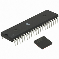
ATMEGA64RZAV-10PU Atmel, ATMEGA64RZAV-10PU Datasheet - Page 128

ATMEGA64RZAV-10PU
Manufacturer Part Number
ATMEGA64RZAV-10PU
Description
MCU ATMEGA644/AT86RF230 40-DIP
Manufacturer
Atmel
Series
ATMEGAr
Datasheets
1.ATMEGA644-20MU.pdf
(23 pages)
2.ATMEGA644-20MU.pdf
(376 pages)
3.AT86RF230-ZU.pdf
(98 pages)
Specifications of ATMEGA64RZAV-10PU
Frequency
2.4GHz
Modulation Or Protocol
802.15.4 Zigbee
Power - Output
3dBm
Sensitivity
-101dBm
Voltage - Supply
1.8 V ~ 3.6 V
Data Interface
PCB, Surface Mount
Memory Size
64kB Flash, 2kB EEPROM, 4kB RAM
Antenna Connector
PCB, Surface Mount
Package / Case
40-DIP (0.600", 15.24mm)
Wireless Frequency
2.4 GHz
Interface Type
JTAG, SPI
Output Power
3 dBm
For Use With
ATSTK600-TQFP32 - STK600 SOCKET/ADAPTER 32-TQFPATAVRISP2 - PROGRAMMER AVR IN SYSTEMATSTK500 - PROGRAMMER AVR STARTER KIT
Lead Free Status / RoHS Status
Lead free / RoHS Compliant
Operating Temperature
-
Applications
-
Data Rate - Maximum
-
Current - Transmitting
-
Current - Receiving
-
Lead Free Status / Rohs Status
Lead free / RoHS Compliant
For Use With/related Products
ATmega64
- Current page: 128 of 376
- Download datasheet (8Mb)
14.11.3
128
ATmega644
TCCR1C – Timer/Counter1 Control Register C
When the ICRn is used as TOP value (see description of the WGMn3:0 bits located in the
TCCRnA and the TCCRnB Register), the ICPn is disconnected and consequently the Input Cap-
ture function is disabled.
• Bit 5 – Reserved Bit
This bit is reserved for future use. For ensuring compatibility with future devices, this bit must be
written to zero when TCCRnB is written.
• Bit 4:3 – WGMn3:2: Waveform Generation Mode
See TCCRnA Register description.
• Bit 2:0 – CSn2:0: Clock Select
The three Clock Select bits select the clock source to be used by the Timer/Counter, see
14-10
Table 14-6.
If external pin modes are used for the Timer/Countern, transitions on the Tn pin will clock the
counter even if the pin is configured as an output. This feature allows software control of the
counting.
• Bit 7 – FOCnA: Force Output Compare for Channel A
• Bit 6 – FOCnB: Force Output Compare for Channel B
The FOCnA/FOCnB bits are only active when the WGMn3:0 bits specifies a non-PWM mode.
However, for ensuring compatibility with future devices, these bits must be set to zero when
TCCRnA is written when operating in a PWM mode. When writing a logical one to the
FOCnA/FOCnB bit, an immediate compare match is forced on the Waveform Generation unit.
The OCnA/OCnB output is changed according to its COMnx1:0 bits setting. Note that the
FOCnA/FOCnB bits are implemented as strobes. Therefore it is the value present in the
COMnx1:0 bits that determine the effect of the forced compare.
Bit
(0x82)
Read/Write
Initial Value
CSn2
0
0
0
0
1
1
1
1
and
Figure
CSn1
0
0
1
1
0
0
1
1
Clock Select Bit Description
FOC1A
R/W
7
0
14-11.
CSn0
FOC1B
0
1
0
1
0
1
0
1
R/W
6
0
Description
No clock source (Timer/Counter stopped).
clk
clk
clk
clk
clk
External clock source on Tn pin. Clock on falling edge.
External clock source on Tn pin. Clock on rising edge.
I/O
I/O
I/O
I/O
I/O
R
5
–
0
/1 (No prescaling)
/8 (From prescaler)
/64 (From prescaler)
/256 (From prescaler)
/1024 (From prescaler)
R
4
–
0
R
3
–
0
R
2
–
0
R
1
–
0
0
–
R
0
2593N–AVR–07/10
TCCR1C
Figure
Related parts for ATMEGA64RZAV-10PU
Image
Part Number
Description
Manufacturer
Datasheet
Request
R

Part Number:
Description:
DEV KIT FOR AVR/AVR32
Manufacturer:
Atmel
Datasheet:

Part Number:
Description:
INTERVAL AND WIPE/WASH WIPER CONTROL IC WITH DELAY
Manufacturer:
ATMEL Corporation
Datasheet:

Part Number:
Description:
Low-Voltage Voice-Switched IC for Hands-Free Operation
Manufacturer:
ATMEL Corporation
Datasheet:

Part Number:
Description:
MONOLITHIC INTEGRATED FEATUREPHONE CIRCUIT
Manufacturer:
ATMEL Corporation
Datasheet:

Part Number:
Description:
AM-FM Receiver IC U4255BM-M
Manufacturer:
ATMEL Corporation
Datasheet:

Part Number:
Description:
Monolithic Integrated Feature Phone Circuit
Manufacturer:
ATMEL Corporation
Datasheet:

Part Number:
Description:
Multistandard Video-IF and Quasi Parallel Sound Processing
Manufacturer:
ATMEL Corporation
Datasheet:

Part Number:
Description:
High-performance EE PLD
Manufacturer:
ATMEL Corporation
Datasheet:

Part Number:
Description:
8-bit Flash Microcontroller
Manufacturer:
ATMEL Corporation
Datasheet:

Part Number:
Description:
2-Wire Serial EEPROM
Manufacturer:
ATMEL Corporation
Datasheet:


