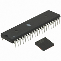
ATMEGA64RZAV-10PU Atmel, ATMEGA64RZAV-10PU Datasheet - Page 253

ATMEGA64RZAV-10PU
Manufacturer Part Number
ATMEGA64RZAV-10PU
Description
MCU ATMEGA644/AT86RF230 40-DIP
Manufacturer
Atmel
Series
ATMEGAr
Datasheets
1.ATMEGA644-20MU.pdf
(23 pages)
2.ATMEGA644-20MU.pdf
(376 pages)
3.AT86RF230-ZU.pdf
(98 pages)
Specifications of ATMEGA64RZAV-10PU
Frequency
2.4GHz
Modulation Or Protocol
802.15.4 Zigbee
Power - Output
3dBm
Sensitivity
-101dBm
Voltage - Supply
1.8 V ~ 3.6 V
Data Interface
PCB, Surface Mount
Memory Size
64kB Flash, 2kB EEPROM, 4kB RAM
Antenna Connector
PCB, Surface Mount
Package / Case
40-DIP (0.600", 15.24mm)
Wireless Frequency
2.4 GHz
Interface Type
JTAG, SPI
Output Power
3 dBm
For Use With
ATSTK600-TQFP32 - STK600 SOCKET/ADAPTER 32-TQFPATAVRISP2 - PROGRAMMER AVR IN SYSTEMATSTK500 - PROGRAMMER AVR STARTER KIT
Lead Free Status / RoHS Status
Lead free / RoHS Compliant
Operating Temperature
-
Applications
-
Data Rate - Maximum
-
Current - Transmitting
-
Current - Receiving
-
Lead Free Status / Rohs Status
Lead free / RoHS Compliant
For Use With/related Products
ATmega64
- Current page: 253 of 376
- Download datasheet (8Mb)
22. JTAG Interface and On-chip Debug System
22.0.1
22.1
22.2
2593N–AVR–07/10
Overview
TAP – Test Access Port
Features
•
•
•
•
•
•
The AVR IEEE std. 1149.1 compliant JTAG interface can be used for
• Testing PCBs by using the JTAG Boundary-scan capability
• Programming the non-volatile memories, Fuses and Lock bits
• On-chip debugging
A brief description is given in the following sections. Detailed descriptions for Programming via
the JTAG interface, and using the Boundary-scan Chain can be found in the sections
ming via the JTAG Interface” on page 303
259, respectively. The On-chip Debug support is considered being private JTAG instructions,
and distributed within ATMEL and to selected third party vendors only.
Figure 22-1
TAP Controller is a state machine controlled by the TCK and TMS signals. The TAP Controller
selects either the JTAG Instruction Register or one of several Data Registers as the scan chain
(Shift Register) between the TDI – input and TDO – output. The Instruction Register holds JTAG
instructions controlling the behavior of a Data Register.
The ID-Register, Bypass Register, and the Boundary-scan Chain are the Data Registers used
for board-level testing. The JTAG Programming Interface (actually consisting of several physical
and virtual Data Registers) is used for serial programming via the JTAG interface. The Internal
Scan Chain and Break Point Scan Chain are used for On-chip debugging only.
The JTAG interface is accessed through four of the AVR’s pins. In JTAG terminology, these pins
constitute the Test Access Port – TAP. These pins are:
• TMS: Test mode select. This pin is used for navigating through the TAP-controller state
• TCK: Test Clock. JTAG operation is synchronous to TCK.
machine.
JTAG (IEEE std. 1149.1 Compliant) Interface
Boundary-scan Capabilities According to the IEEE std. 1149.1 (JTAG) Standard
Debugger Access to:
Extensive On-chip Debug Support for Break Conditions, Including
Programming of Flash, EEPROM, Fuses, and Lock Bits through the JTAG Interface
On-chip Debugging Supported by AVR Studio
– All Internal Peripheral Units
– Internal and External RAM
– The Internal Register File
– Program Counter
– EEPROM and Flash Memories
– AVR Break Instruction
– Break on Change of Program Memory Flow
– Single Step Break
– Program Memory Break Points on Single Address or Address Range
– Data Memory Break Points on Single Address or Address Range
shows a block diagram of the JTAG interface and the On-chip Debug system. The
and
®
”IEEE 1149.1 (JTAG) Boundary-scan” on page
ATmega644
”Program-
253
Related parts for ATMEGA64RZAV-10PU
Image
Part Number
Description
Manufacturer
Datasheet
Request
R

Part Number:
Description:
DEV KIT FOR AVR/AVR32
Manufacturer:
Atmel
Datasheet:

Part Number:
Description:
INTERVAL AND WIPE/WASH WIPER CONTROL IC WITH DELAY
Manufacturer:
ATMEL Corporation
Datasheet:

Part Number:
Description:
Low-Voltage Voice-Switched IC for Hands-Free Operation
Manufacturer:
ATMEL Corporation
Datasheet:

Part Number:
Description:
MONOLITHIC INTEGRATED FEATUREPHONE CIRCUIT
Manufacturer:
ATMEL Corporation
Datasheet:

Part Number:
Description:
AM-FM Receiver IC U4255BM-M
Manufacturer:
ATMEL Corporation
Datasheet:

Part Number:
Description:
Monolithic Integrated Feature Phone Circuit
Manufacturer:
ATMEL Corporation
Datasheet:

Part Number:
Description:
Multistandard Video-IF and Quasi Parallel Sound Processing
Manufacturer:
ATMEL Corporation
Datasheet:

Part Number:
Description:
High-performance EE PLD
Manufacturer:
ATMEL Corporation
Datasheet:

Part Number:
Description:
8-bit Flash Microcontroller
Manufacturer:
ATMEL Corporation
Datasheet:

Part Number:
Description:
2-Wire Serial EEPROM
Manufacturer:
ATMEL Corporation
Datasheet:


