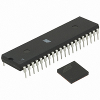
ATMEGA64RZAV-10PU Atmel, ATMEGA64RZAV-10PU Datasheet - Page 105

ATMEGA64RZAV-10PU
Manufacturer Part Number
ATMEGA64RZAV-10PU
Description
MCU ATMEGA644/AT86RF230 40-DIP
Manufacturer
Atmel
Series
ATMEGAr
Datasheets
1.ATMEGA644-20MU.pdf
(23 pages)
2.ATMEGA644-20MU.pdf
(376 pages)
3.AT86RF230-ZU.pdf
(98 pages)
Specifications of ATMEGA64RZAV-10PU
Frequency
2.4GHz
Modulation Or Protocol
802.15.4 Zigbee
Power - Output
3dBm
Sensitivity
-101dBm
Voltage - Supply
1.8 V ~ 3.6 V
Data Interface
PCB, Surface Mount
Memory Size
64kB Flash, 2kB EEPROM, 4kB RAM
Antenna Connector
PCB, Surface Mount
Package / Case
40-DIP (0.600", 15.24mm)
Wireless Frequency
2.4 GHz
Interface Type
JTAG, SPI
Output Power
3 dBm
For Use With
ATSTK600-TQFP32 - STK600 SOCKET/ADAPTER 32-TQFPATAVRISP2 - PROGRAMMER AVR IN SYSTEMATSTK500 - PROGRAMMER AVR STARTER KIT
Lead Free Status / RoHS Status
Lead free / RoHS Compliant
Operating Temperature
-
Applications
-
Data Rate - Maximum
-
Current - Transmitting
-
Current - Receiving
-
Lead Free Status / Rohs Status
Lead free / RoHS Compliant
For Use With/related Products
ATmega64
- Current page: 105 of 376
- Download datasheet (8Mb)
14.2.1
2593N–AVR–07/10
Registers
Figure 14-1. 16-bit Timer/Counter Block Diagram
Note:
The Timer/Counter (TCNTn), Output Compare Registers (OCRnA/B/C), and Input Capture Reg-
ister (ICRn) are all 16-bit registers. Special procedures must be followed when accessing the 16-
bit registers. These procedures are described in the section
page
CPU access restrictions. Interrupt requests (abbreviated to Int.Req. in the figure) signals are all
visible in the Timer Interrupt Flag Register (TIFRn). All interrupts are individually masked with
the Timer Interrupt Mask Register (TIMSKn). TIFRn and TIMSKn are not shown in the figure.
The Timer/Counter can be clocked internally, via the prescaler, or by an external clock source on
the Tn pin. The Clock Select logic block controls which clock source and edge the Timer/Counter
uses to increment (or decrement) its value. The Timer/Counter is inactive when no clock source
is selected. The output from the Clock Select logic is referred to as the timer clock (clk
The double buffered Output Compare Registers (OCRnA/B/C) are compared with the
Timer/Counter value at all time. The result of the compare can be used by the Waveform Gener-
ator to generate a PWM or variable frequency output on the Output Compare pin (OCnA/B/C).
106. The Timer/Counter Control Registers (TCCRnA/B/C) are 8-bit registers and have no
Refer to
placement and description.
Figure 1-1 on page 2
Timer/Counter
TCCRnA
OCRnA
OCRnB
TCNTn
ICRn
=
=
Direction
Count
Clear
and
”Alternate Port Functions” on page 71
Control Logic
TOP
=
TCCRnB
Values
BOTTOM
Fixed
TOP
ICFn (Int.Req.)
(Note:)
clk
Detector
Edge
=
Tn
0
”Accessing 16-bit Registers” on
OCnA
(Int.Req.)
OCnB
(Int.Req.)
TOVn
(Int.Req.)
Clock Select
Generation
Generation
( From Prescaler )
Waveform
Waveform
Canceler
Detector
Noise
Edge
ATmega644
for Timer/Counter1 pin
Comparator Ouput )
( From Analog
T
OCnB
OCnA
ICPn
n
Tn
).
105
Related parts for ATMEGA64RZAV-10PU
Image
Part Number
Description
Manufacturer
Datasheet
Request
R

Part Number:
Description:
DEV KIT FOR AVR/AVR32
Manufacturer:
Atmel
Datasheet:

Part Number:
Description:
INTERVAL AND WIPE/WASH WIPER CONTROL IC WITH DELAY
Manufacturer:
ATMEL Corporation
Datasheet:

Part Number:
Description:
Low-Voltage Voice-Switched IC for Hands-Free Operation
Manufacturer:
ATMEL Corporation
Datasheet:

Part Number:
Description:
MONOLITHIC INTEGRATED FEATUREPHONE CIRCUIT
Manufacturer:
ATMEL Corporation
Datasheet:

Part Number:
Description:
AM-FM Receiver IC U4255BM-M
Manufacturer:
ATMEL Corporation
Datasheet:

Part Number:
Description:
Monolithic Integrated Feature Phone Circuit
Manufacturer:
ATMEL Corporation
Datasheet:

Part Number:
Description:
Multistandard Video-IF and Quasi Parallel Sound Processing
Manufacturer:
ATMEL Corporation
Datasheet:

Part Number:
Description:
High-performance EE PLD
Manufacturer:
ATMEL Corporation
Datasheet:

Part Number:
Description:
8-bit Flash Microcontroller
Manufacturer:
ATMEL Corporation
Datasheet:

Part Number:
Description:
2-Wire Serial EEPROM
Manufacturer:
ATMEL Corporation
Datasheet:


