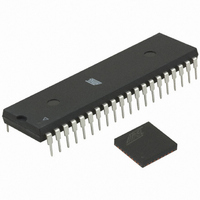
ATMEGA64RZAV-10PU Atmel, ATMEGA64RZAV-10PU Datasheet - Page 177

ATMEGA64RZAV-10PU
Manufacturer Part Number
ATMEGA64RZAV-10PU
Description
MCU ATMEGA644/AT86RF230 40-DIP
Manufacturer
Atmel
Series
ATMEGAr
Datasheets
1.ATMEGA644-20MU.pdf
(23 pages)
2.ATMEGA644-20MU.pdf
(376 pages)
3.AT86RF230-ZU.pdf
(98 pages)
Specifications of ATMEGA64RZAV-10PU
Frequency
2.4GHz
Modulation Or Protocol
802.15.4 Zigbee
Power - Output
3dBm
Sensitivity
-101dBm
Voltage - Supply
1.8 V ~ 3.6 V
Data Interface
PCB, Surface Mount
Memory Size
64kB Flash, 2kB EEPROM, 4kB RAM
Antenna Connector
PCB, Surface Mount
Package / Case
40-DIP (0.600", 15.24mm)
Wireless Frequency
2.4 GHz
Interface Type
JTAG, SPI
Output Power
3 dBm
For Use With
ATSTK600-TQFP32 - STK600 SOCKET/ADAPTER 32-TQFPATAVRISP2 - PROGRAMMER AVR IN SYSTEMATSTK500 - PROGRAMMER AVR STARTER KIT
Lead Free Status / RoHS Status
Lead free / RoHS Compliant
Operating Temperature
-
Applications
-
Data Rate - Maximum
-
Current - Transmitting
-
Current - Receiving
-
Lead Free Status / Rohs Status
Lead free / RoHS Compliant
For Use With/related Products
ATmega64
- Current page: 177 of 376
- Download datasheet (8Mb)
17.7.6
17.7.7
17.8
17.8.1
2593N–AVR–07/10
Asynchronous Data Reception
Disabling the Receiver
Flushing the Receive Buffer
Asynchronous Clock Recovery
with the received data and stop bits. The Parity Error (UPEn) Flag can then be read by software
to check if the frame had a Parity Error.
The UPEn bit is set if the next character that can be read from the receive buffer had a Parity
Error when received and the Parity Checking was enabled at that point (UPMn1 = 1). This bit is
valid until the receive buffer (UDRn) is read.
In contrast to the Transmitter, disabling of the Receiver will be immediate. Data from ongoing
receptions will therefore be lost. When disabled (that is, the RXENn is set to zero) the Receiver
will no longer override the normal function of the RxDn port pin. The Receiver buffer FIFO will be
flushed when the Receiver is disabled. Remaining data in the buffer will be lost
The receiver buffer FIFO will be flushed when the Receiver is disabled, that is, the buffer will be
emptied of its contents. Unread data will be lost. If the buffer has to be flushed during normal
operation, due to for instance an error condition, read the UDRn I/O location until the RXCn Flag
is cleared. The following code example shows how to flush the receive buffer.
Note:
The USART includes a clock recovery and a data recovery unit for handling asynchronous data
reception. The clock recovery logic is used for synchronizing the internally generated baud rate
clock to the incoming asynchronous serial frames at the RxDn pin. The data recovery logic sam-
ples and low pass filters each incoming bit, thereby improving the noise immunity of the
Receiver. The asynchronous reception operational range depends on the accuracy of the inter-
nal baud rate clock, the rate of the incoming frames, and the frame size in number of bits.
The clock recovery logic synchronizes internal clock to the incoming serial frames.
illustrates the sampling process of the start bit of an incoming frame. The sample rate is 16 times
the baud rate for Normal mode, and eight times the baud rate for Double Speed mode. The hor-
izontal arrows illustrate the synchronization variation due to the sampling process. Note the
Assembly Code Example
C Code Example
USART_Flush:
void USART_Flush( void )
{
}
sbis UCSRnA, RXCn
ret
in
rjmp USART_Flush
unsigned char dummy;
while ( UCSRnA & (1<<RXCn) ) dummy = UDRn;
1. See “About Code Examples” on page 8.
r16, UDRn
(1)
(1)
ATmega644
Figure 17-5
177
Related parts for ATMEGA64RZAV-10PU
Image
Part Number
Description
Manufacturer
Datasheet
Request
R

Part Number:
Description:
DEV KIT FOR AVR/AVR32
Manufacturer:
Atmel
Datasheet:

Part Number:
Description:
INTERVAL AND WIPE/WASH WIPER CONTROL IC WITH DELAY
Manufacturer:
ATMEL Corporation
Datasheet:

Part Number:
Description:
Low-Voltage Voice-Switched IC for Hands-Free Operation
Manufacturer:
ATMEL Corporation
Datasheet:

Part Number:
Description:
MONOLITHIC INTEGRATED FEATUREPHONE CIRCUIT
Manufacturer:
ATMEL Corporation
Datasheet:

Part Number:
Description:
AM-FM Receiver IC U4255BM-M
Manufacturer:
ATMEL Corporation
Datasheet:

Part Number:
Description:
Monolithic Integrated Feature Phone Circuit
Manufacturer:
ATMEL Corporation
Datasheet:

Part Number:
Description:
Multistandard Video-IF and Quasi Parallel Sound Processing
Manufacturer:
ATMEL Corporation
Datasheet:

Part Number:
Description:
High-performance EE PLD
Manufacturer:
ATMEL Corporation
Datasheet:

Part Number:
Description:
8-bit Flash Microcontroller
Manufacturer:
ATMEL Corporation
Datasheet:

Part Number:
Description:
2-Wire Serial EEPROM
Manufacturer:
ATMEL Corporation
Datasheet:


